Scientists make detailed map of current between insulators

When scientists found electrical current flowing where it shouldn't be – at the place where two insulating materials meet– it set off a frenzy of research that turned up more weird properties and the hope of creating a new class of electronics.
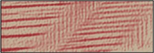
Now SLAC and Stanford scientists have mapped those currents in microscopic detail and found another surprise: Rather than flowing uniformly, the currents are stronger in some places than others, like river currents shaped by underlying rock.
Their finding, published Sunday in Nature Materials, is an important step in understanding why these two materials – lanthanum aluminate and strontium titanate (LAO and STO for short) – dramatically change behavior when sandwiched together.
It looks like the currents at the interface are shaped by subtle distortions in the crystalline structure of the STO layer, said Kathryn A. "Kam" Moler of the Stanford Institute for Materials and Energy Sciences (SIMES), who led the research team. The cube-shaped arrangement of the atoms in the structure stretches when chilled, and variations in the direction of that stretching from one tiny region to another seem to channel the current flow.
But it will take more digging to pin down what is happening at the atomic level, she said. The team hopes to do those studies at SLAC's Stanford Synchrotron Radiation Lightsource, which generates brilliant X-ray beams for probing atomic structure.
"I think it's interesting that LAO/STO is a very well-studied system, but this effect was never expected," said Eric M. Spanton, a SLAC graduate student on the research team. "By understanding what is happening in the regions where the current flows stronger, maybe we can figure out how to make the whole sample conduct better."
The more scientists understand how materials operate at the scale of individual atoms, the better they can design them with exactly the properties they want, said Harold Hwang, a professor at SLAC and Stanford who was part of the research team.
It was Hwang and a colleague who in 2004 discovered currents flowing at the interface between LAO and STO. Three years later, another group showed that when the layers are chilled, the interface becomes superconducting; that is, it conducts electricity with zero resistance and 100 percent efficiency. Yet another group found that magnetism could exist in the gap, even though neither of the layers is inherently magnetic. And in 2011, Moler, Hwang and colleagues, along with a separate group at MIT, announced an even more improbable finding: The chilled interface can contain superconducting regions and magnetic regions at the same time. The two aren't supposed to coexist.
Today's devices use several types of switches to control the flow of information. Changes in voltage are used to switch transistors that guide the flow of current on computer chips. Changes in magnetism operate switches that store information on hard drives, and electric switches store data on flash drives. The promise of the LAO/STO interface – one of a class of materials known as engineered heterostructures – is that it might allow two or three types of switches to operate in a single device.
"The hope is you would be able to get more stuff into a smaller space and switch it faster using less energy," Moler said, "but that's all very speculative."
For the latest study, much of the work was carried out by Spanton and Beena Kalisky, a SIMES postdoctoral researcher who left midway through to take a faculty position at Bar-Ilan University in Israel.
They would put a sample of the LAO/STO sandwich into a vacuum chamber, run an electrical current through it and use an exquisitely sensitive device called a SQUID to measure the magnetic field the current induced. Those measurements showed the current was stronger in some places and weaker in others, creating striped patterns. Kalisky then used a polarized light microscope to map out the underlying patterns of structural distortion in the STO layer.
More information: Nature Materials (2013) DOI: 10.1038/nmat3753
Journal information: Nature Materials
Provided by SLAC National Accelerator Laboratory


