May 28, 2013 feature
Metallic-to-semiconducting nanotube conversion greatly improves transistor performance

(Phys.org) —Future transistors made of semiconducting single-walled carbon nanotubes (s-SWNTs) have the potential to perform much better than today's transistors. However, when SWNTs are grown in bulk, only about two-thirds of them are semiconducting, while the other one-third are metallic (m-SWNTs). Since m-SWNTs have a higher conductivity than s-SWNTs, their presence allows current leakage in a transistor's off state, which greatly decreases the transistor's on/off current ratio and overall performance. In a new study, scientists have demonstrated that simply decorating the m-SWNTs with copper oxide nanoparticles can convert them into s-SWNTs, resulting in a 205-fold increase in a transistor's on/off current ratio.
The researchers, Darya Asheghali, Pornnipa Vichchulada, and Associate Professor Marcus D. Lay at the University of Georgia in Athens, have published their paper on converting m-SWNTs to s-SWNTs in a recent issue of the Journal of the American Chemical Society.
Previous studies have attempted to overcome the problem of m-SWNTs by using methods that are often complex and expensive. Some approaches involve using specialized SWNT growth methods that select for s-SWNTs, while other approaches involve post-growth solution processing to remove m-SWNTs.
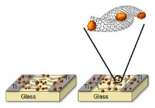
The approach proposed in the new study could provide a simpler solution to obtain large amounts of s-SWNTs. After growing the SWNTs using a conventional bulk growth method, the researchers deposited sub-10-nm copper oxide nanoparticles on all of the nanotubes, both metallic and semiconducting. This single step converts the m-SWNTs into s-SWNTs and also improves the electric properties of the original s-SWNTs.
When the researchers incorporated these decorated s-SWNTs into transistors, they found that the transistors' on/off current ratios increased from about 21 to 4300, representing a 205-fold improvement.
The reason that the nanoparticles have this effect is because of the way they change the SWNTs' band gaps. Since a band gap is the energy range in a material where electrons cannot exist, generally a large band gap corresponds to low electrical conductivity, and vice versa. Typically, insulators have large band gaps, semiconductors have smaller band gaps, and conductors have very small or no band gaps.
In the current study, the m-SWNTs originally have no band gap, making them good conductors. Although high conductivity is good when transistors are in the on state (when electrons flow), it is a liability in the off state (where electrons don't flow). Being highly conductive, the m-SWNTs leak a lot of current in the off state.
As the researchers demonstrate here, the copper oxide nanoparticles can open up a band gap in the m-SWNTs, which restricts the current flow and greatly reduces the leakage current when the transistor is in the off state. Now that the m-SWNTs have a band gap, they are by definition s-SWNTs. The nanoparticles also increase the band gaps of the s-SWNTs, which improves both their uniformity and current efficiency.
The researchers explain that the copper oxide nanoparticles create/increase these band gaps by withdrawing electron density from the SWNTs at the point of contact. In a sense, the nanoparticles act like tiny valves along a wire that increase the SWNTs' sensitivity to gate voltages at certain points, changing the conductivity of the SWNTs overall.
Although the researchers describe the effect as a conversion of metallic SWNTs to semiconducting SWNTs, they also clarify that, when it comes down to it, m-SWNTs are not true metals. Instead, they should be considered semimetals or zero band gap semiconductors because true metals could not be made sensitive to the gate voltage.
Graphene also falls into this category of semimetals. However, it is more complicated to open a band gap in graphene because graphene is a 2-D material. The researchers explain that the 1-D nature of SWNTs simplifies the process of band gap tuning by allowing the nanoparticles to act like valves on a wire and locally halt electron transport. This approach cannot carry over to planar graphene due do its different geometry.
This relatively simple method of using nanoparticles to convert m-SWNTs into s-SWNTs, and the significant performance improvement that results, has great potential to further the development of SWNT-based transistors in the future, as well as carry over to other areas.
"The ability to open a bandgap in graphite-based semiconductors like SWNTs and graphene will have applications in sensors and energy conversion," Lay told Phys.org.
As for SWNT field-effect transistors (FETs), Lay explained that other challenges remain before they can become commercially widespread.
"The biggest problem facing SWNT FETs is the dearth of purification and suspension formation methods that separate the high aspect ratio SWNTs needed for structural and electronic applications from the soot and catalyst particles that make up about 50% of SWNT samples with common bulk growth methods," he said. "Another major roadblock is the lack of deposition methods that allow control over the density and alignment of SWNTs."
Lay and his group have contributed significantly to these two areas in another recent study1.
More information: D. Asheghali, P. Vichchulada, and M. D. Lay. "Conversion of Metallic Single-Walled Carbon Nanotube Networks to Semiconducting through Electrochemical Ornamentation." J. Am. Chem. Soc., 2013, 135 (20), 7511–7522. DOI: 10.1021/ja311721g
Note:
1 N. P. Bhatt, P. Vichchulada, and M. D. Lay. "Bulk Purification and Deposition Methods for Selective Enrichment in High Aspect Ratio Single-Walled Carbon Nanotubes." J. Am. Chem. Soc., 134 (2012) 9352-9361, DOI: 10.1021/ja302136x
Journal information: Journal of the American Chemical Society
© 2013 Phys.org. All rights reserved.


