Bringing all-optical networks closer to home
Converting between electronic and optical signals is one of the main costs in high-speed data networks and telecommunications applications, even more so when looking at future applications. The solution, say the experts, is to introduce cost-competitive and effective all-optical circuits to reduce the load on electronics.
Introducing all-optical circuits is exactly what one European research group has done. The driving force behind the research is the ever-faster data transfer rates demanded by network and telecommunications systems.
The astronomical growth of data networks in recent decades, whether connecting homes, businesses or whole cities, has been made possible not only because researchers developed increasingly faster ways of sending information over copper wires and optic cables; but also because the network components, the cabling, the laser transmitters, the switches and the filters have been available in larger quantities and at acceptable prices.
A conversion bottleneck
Today, fast data transfer rates of tens of gigabits per second (Gb/s) are achieved by using hybrid optical/electrical systems to handle the data. High-capacity optic fibres are used to transfer data across the network, between countries, across regions and from office to office. But at several points along the network, the optical signals (photons) are converted to electrical signals to recover the data, clean it up, determine where it came from, decide where it is going, and deliver it.
Yet the demand for more and faster data communications – more bandwidth – is growing exponentially as more users go online to use increasingly sophisticated services and applications. Consumers want video, television and interactive applications at home, businesses want to store and access huge corporate data banks remotely, and scientists want more powerful, distributed computing.
However, the present need to convert optical data into electrical signals is a critical bottleneck to obtaining faster data communications. This is where the EU-funded MUFINS – Multi-functional integrated arrays of interferometric switches – project comes in.
Price matters
“At data rates of up to 10 Gb/s, electrons can still do the job, but the electronics are getting expensive once we reach 40 Gb/s and above,” explains MUFINS researcher George Theophilopoulos of the Research Academic Computer Technology Institute (RACTI). A conclusion highlighted by techno-economic studies performed by Telecom Italia and Nokia-Siemens, two other project partners.
“All-optical systems”, he continues, “are needed because, at these rates, electronic solutions are too complex, too expensive and have huge power dissipation and thermal problems – they are reaching their physical limits; or will soon be.”
However, although researchers in the past have made progress in producing the optical hardware, such as switches and receivers that all-optical networks need, they were simply too expensive for commercial applications because they were custom-made, one at a time. This critical cost issue is the challenge that MUFINS’ researchers are tackling.
“Using monolithic and hybrid fabrication techniques, we integrated several optical elements, such as interferometric switches, on the same chip substrate. This means that the packaging and pigtailing costs are shared between them,” says Theophilopoulos.
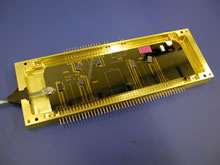
One MUFINS partner, the Centre for Integrated Photonics (CIP), designed, fabricated and packaged four-element, 40 Gb/s optical switches – the equivalent of transistors in electronic circuits – on the same substrate, using hybrid photonic integration manufacturing. Two other partners, the Technical University of Eindhoven and the University of Bristol, used monolithic processes, like those used in chip manufacturing, to produce similar devices operating at 40 Gb/s.
“The significant achievement here,” stresses Theophilopoulos “is that they integrated four elementary switches on the same device, so the cost per device is cut almost by a factor of four!”
Jewel in the crown
By using the CIP optical devices, the project successfully demonstrated numerous complex and diverse optical experiments up to 40 Gb/s, incorporating simultaneously up to 12 switching elements. For example, MUFINS coordinator RACTI demonstrated a four-wavelength Burst Mode Receiver (BMR); the Heinrich-Hertz-Institut showed successful operation of a half- and a full-adder circuit, the Technical University of Eindhoven produced a data vortex switch and a 4x4 switching matrix, while the University of Essex characterised MUFINS devices in a complex network topology. However, the jewel in the crown for the MUFINS researchers is their integrated all-optical BMR operating at 40 Gb/s.
“[These receivers] are used at the end of optical fibres to acquire and regenerate asynchronous data packets, so they are a vital part of any optical network,” explains Theophilopoulos. They had been demonstrated experimentally in laboratories by connecting up many discrete components. But at the end of the project, CIP developed a BMR device that is manufactured on a single chip using low-cost scalable production processes.
“This is one of the most complex all-optical circuits ever developed,” Theophilopoulos tells ICT Results, “with many potential commercial applications in ultra-high-speed optical networks, and the potential for cost reduction is inherent in the fabrication process we used.”
Desirable devices
The true success of the MUFINS project is found not only in the new devices and fabrication processes it developed. It is also seen in the demand for their unique devices from researchers worldwide. “It is the first time I have heard of a new device leaving the lab and heading straight to the researchers and R&D engineers in major universities, research institutes and telecommunications companies worldwide,“ says Theophilopoulos.
But that is what is happening. More than 50 MUFINS-technology switches have already been supplied by CIP to research groups, he reports, attracted by the prospect of affordable devices, available in numbers and with a potential low cost in large volumes – just what is needed to get all-optical networks off the ground.
Source: ICT Results


