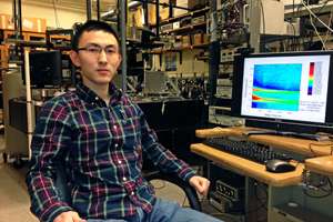
A new twist on a very old physics technique could impact nanoscience

(Phys.org) —A new twist on a very old physics technique could have a profound impact on one of the most buzzed-about aspects of nanoscience.
Researchers at the University of Cincinnati have found that their unique method of light-matter interaction analysis appears to be a good way of helping make better semiconductor nanowires.
"Semiconductor nanowires are one of the hottest topics in the nanoscience research field in the recent decade," says Yuda Wang, a UC doctoral student. "Due to the unique geometry compared to conventional bulk semiconductors, nanowires have already shown many advantageous properties, particularly in novel applications in such fields as nanoelectronics, nanophotonics, nanobiochemistry and nanoenergy."
Wang will present the team's research "Transient Rayleigh Scattering Spectroscopy Measurement of Carrier Dynamics in Zincblende and Wurtzite Indium Phosphide Nanowires" at the American Physical Society (APS) meeting to be held March 3-7 in Denver. Nearly 10,000 professionals, scholars and students will attend the APS meeting to discuss new research from industry, universities and laboratories from around the world.
Key to this research is UC's new method of Rayleigh scattering, a phenomenon first described in 1871 and the scientific explanation for why the sky is blue in the daytime and turns red at sunset. The researchers' Rayleigh scattering technique probes the band structures and electron-hole dynamics inside a single indium phosphide nanowire, allowing them to observe the response with a time resolution in the femtosecond range – or one quadrillionth of a second.
"Basically, we can generate a live picture of how the electrons and holes are excited and slowly return to their original states, and the mechanism behind that can be analyzed and understood," says Wang, of UC's Department of Physics. "It's all critical in characterizing the optical or electronic properties of a semiconducting nanowire."
Semiconductors are at the center of modern electronics. Computers, TVs and cellphones have them. They're made from the crystalline form of elements that have scientifically beneficial electrical conductivity properties.
Wang says the burgeoning range of semiconductor nanowire applications – such as smaller, more energy-efficient electronics – has brought rapid improvement to nanowire fabrication techniques. He says his team's research could offer makers of nanotechnology a new and highly effective option for measuring the physics inside nanowires.
"The key to a good optimization process is an excellent feedback, or a characterization method," Wang says. "Rayleigh scattering appears to be an exceptional way to measure several nanowire properties simultaneously in a non-invasive and high-quality manner."
Provided by University of Cincinnati


