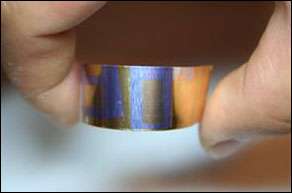
Testing, Radiation Testing: Northwestern Transistors On Space Station

Transistors based on a new kind of material created by Northwestern University researchers have been lifted into outer space on the space shuttle Endeavour and attached to the outside of the International Space Station for radiation testing.
Such transistors could prove helpful on long space missions, such as NASA’s current Phoenix Mars Mission, since early experiments on Earth indicate that the transistors hold up well when exposed to radiation.
The transistors, which used a new kind of gate dielectric material called a self-assembled nanodielectric (SAND), were placed on the space station during a spacewalk March 22. The transistors will remain there for a year as part of a NASA materials experiment to see how they and other materials hold up to the harsh space environment.
SANDs were developed at Northwestern by the research group of Tobin Marks, Vladimir N. Ipatieff Research Professor of Chemistry in the Weinberg College of Arts and Sciences and Professor of Materials Science and Engineering in the McCormick School of Engineering and Applied Science. Marks says that, in addition to possibly proving handy in space, SANDs could help pave the way for a variety of new technologies, including printable and transparent electronics.
Transistors, the devices used to amplify or switch signals that are the building blocks of all modern electronic devices, generally consist of a substrate, gate and semiconductor. In between the gate and semiconductor lies the dielectric, which acts as an insulator to prevent short circuiting while stabilizing charged current carriers in the nearby semiconductor.
While silicon dioxide has historically been the dominant dielectric material for silicon-based electronics, Marks and his research group have been trying to create next-generation semiconductor and dielectric materials with properties that silicon and silicon dioxide can’t provide -- such as transparency, printability and physical flexibility. The dielectric material would need to be thin, be a good insulator and be able to stabilize the charges moving through the semiconductor by having what is called a high dielectric constant, which is the relative ability of the material to store an electric charge for a given applied field strength.
What resulted were SANDs, which Marks and his team created through a dipping process that creates self-assembled molecular thin films. Not only do SANDs meet all the requirements for next-generation dielectrics, but they were also found to be resistant to radiation.
NASA is interested in SANDs because the radiation in space severely damages electronics -- especially dielectrics, since silicon dioxide captures the radiation, which then forms holes and electrons and irreversibly builds up a destructive charge in the transistor. For long space trips -- like the current mission to Mars -- such electronics are exposed to years of radiation. Early tests with nuclear reactors showed that SANDs are largely resistant to such radiation damage.
“Everybody was astounded,” Marks says. “These experiments showed that SANDs have the potential to revolutionize the whole field.”
Marks and his team will have an even better idea of how the SAND transistors fare after they remain on the space station for a year. In the meantime, they hope to continue to improve upon the transistors, making better semiconductors with thinner dielectrics and even higher dielectric constants. In a paper published online May 3 in the Journal of the American Chemical Society with colleagues Mark Ratner, Antonio Facchetti, Sara DiBenedetto and David Frattarelli, the team showed that SAND-type materials can be made through vapor deposition, a common process used in the semiconductor industry to produce thin films.
While SANDs could help researchers explore the final frontier, Marks and his group will continue to work toward technologies that will benefit everyone on Earth, such as the ability to print transistors like newspapers, making way for cheaper, more durable electronics.
“It’s not just that these transistors are only good for outer space -- that’s an illustration of just how tough they are,” Marks says. “There is one technology on Earth, and only one, that will create as many features per unit time as a chip plant, and that’s a modern newspaper printing plant, since the paper flies at hundreds of feet per second. Every time Intel wants to make a new chip, it costs billions of dollars and takes years to do. And yet every day they print a new New York Times. So we thought, could you use printing to create electronic circuits?”
Such a technology could print large items like solar cells and flat-panel displays, as well as small items, like circuits for cell phones and medical equipment. One of the long-range goals is to print radio frequency ID tags for items for sale in a store, which could provide information on the item’s price, where it was manufactured, how it was made and how it was stored. It would also allow a cashier to zap a shopper’s entire basket in one go, instead of scanning bar codes one-by-one.
“It’s like the tollway iPass for packages,” Marks says. “A bell could go off and say, no, that’s expired or it could tell a central computer that the store is almost out of an item.”
Another development from such technology could be transparent electronics, which could provide new items like decals that could be applied to a car windshield that would instantaneously show the car’s speed, fuel level and other dashboard information.
Some cell phones on the market already have printed electronics inside, and Marks and his group have already created printed circuits with the team’s materials. The group is continuing to make transistor materials into inks in order to make printed electronics an everyday reality.
Source: Northwestern University


