Researchers improve method for probing semiconducting crystals with light to detect defects and impurities

Tohoku University researchers have improved a method for probing semiconducting crystals with light to detect defects and impurities. The details of their omnidirectional photoluminescence (ODPL) spectroscopy set-up were published in the journal Applied Physics Express, and could help improve the fabrication of materials for electric cars and solar cells.
"Our technique can test materials at very low temperatures and can find even small amounts of defects and impurities," says Tohoku University materials scientist Kazunobu Kojima.
Kojima and his colleagues demonstrated their approach using gallium nitride crystals. Gallium nitride is a semiconducting crystal that has been used in energy-saving light-emitting diodes (LEDs) since the 2000s. It has interesting optic and electronic properties, making it attractive for many applications, including power-switching devices in electric vehicles. But it can develop defects and impurities during its fabrication, which can affect performance. Currently available methods for testing these crystals are expensive or too invasive.
The ODPL spectroscopy, on the other hand, is a non-invasive technique that can test the crystals, but only at room temperature. Being able to change the crystal's temperature is important to properly test its properties.
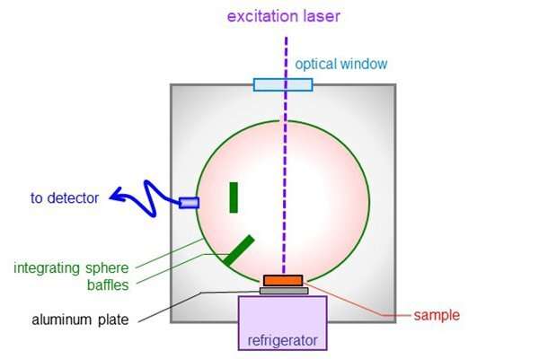
Kojima and his colleagues found a way to set up an ODPL instrument so that the crystal can be cooled. The process involves placing a gallium nitride crystal on an aluminum plate connected to a cooling device. This is placed under an "integrating sphere," which collects light coming from many directions. External light is shone through the sphere onto the crystal, exciting it. The crystal emits light back into the sphere in order to return to its initial unexcited state. The two lights, from the external source and the crystal, are integrated within the sphere and measured by a detector. The result reveals the crystal's "internal quantum efficiency," which is reduced if it contains defects and impurities, and can be measured even at very low temperatures.
The team's modification—placing the crystal outside the sphere and connecting it to something that cools it—means the temperature change crucially happens only within the crystal and not within the sphere. The scientists were able to measure the internal quantum efficiency of gallium nitride samples using this technique at temperatures ranging from -261°C to about 27°C.
"We next plan to use our method for testing other materials, such as perovskites for use in highly efficient solar cells and boron nitride as an atomically thin two-dimensional material," says Kojima.
More information: Kazunobu Kojima et al. Temperature dependence of internal quantum efficiency of radiation for the near-band-edge emission of GaN crystals quantified by omnidirectional photoluminescence spectroscopy, Applied Physics Express (2020). DOI: 10.35848/1882-0786/abb788
Provided by Tohoku University


