Breakthrough in spintronics

It's ultra-thin, electrically conducting at the edge and highly insulating within—and all that at room temperature: Physicists from the University of Würzburg have developed a promising new material.
The material class of topological insulators is presently the focus of international solids research. These materials are electrically insulating within, because the electrons maintain strong bonds to the atoms. At their surfaces, however, they are conductive due to quantum effects.
Additionally, the electron's spin orientation is capable of transmitting information very efficiently. It is protected against scattering when moving through these surface channels. With these properties, topological insulators could make an old dream come true—direct spin-based data processing, or so-called spintronics.
Previous concepts only work in the refrigerator
Until now, however, there has been one major obstacle to using such surface channels for technical applications: "As the temperature of a topological insulator increases, all quantum effects are washed out and with them, the special properties of the electrically conducting edges," Dr Jörg Schäfer explains; he is a private lecturer at the Chair of Experimental Physics 4 of the University of Würzburg.
For this reason, all known topological insulators have to be cooled to very low temperatures—usually down to minus 270 degrees Celsius—to be able to study the quantum properties of the edge channels. "Of course, such conditions are not very practicable for potential applications such as ultra-fast electronics or quantum computers," the physicist says.
A team of Würzburg physicists has now presented an entirely new concept to elegantly bypass this problem. The scientists have published their results in the current issue of Science.
Targeted material design
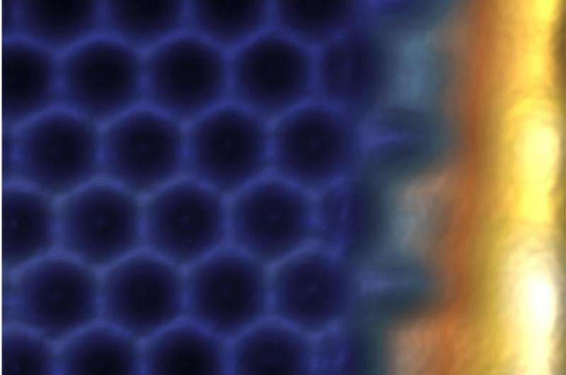
The Würzburg breakthrough is based on a special combination of materials: an ultra-thin film consisting of a single layer of bismuth atoms deposited on a silicon carbide substrate.
What makes this combination so special? "The crystalline structure of the silicon carbide substrate causes the bismuth atoms to arrange in a honeycomb geometry when depositing the bismuth film—very similar to the structure of the 'miracle material' graphene, which is made up of carbon atoms", Professor Ralph Claessen explains. Because of this analogy, the waver-thin film is called "bismuthene".
But it has one decisive difference compared to graphene: "Bismuthene forms a chemical bond to the substrate," Professor Ronny Thomale says. It plays a central role in the new concept to provide the material with the desired electronic properties. This is highlighted by computer-based modelling: "Whereas common bismuth is an electrically conductive metal, the honeycomb monolayer remains a distinct insulator, even at room temperature and far above," the physicist adds. To create this much-desired initial condition artificially, the heavy bismuth atoms are ingeniously combined with the equally insulating silicon-carbide substrate.
Electron motorway on the edge
The electronic conduction channels come into play at the edge of a piece of bismuthene. This is where the metallic edge channels are located, which are to be used for the data processing of the future. This has not only been concluded theoretically by the Würzburg research team, it has also been proven in experiments using microscopic techniques.
In order to harness the edge channels for electronic components, it is crucial that there is no short-circuit through the inside of the topological material or through the substrate. "Previous topological insulators required extreme cooling to assure this," Jörg Schäfer explains. The new bismuthene concept makes this effort redundant: The distinct insulating behaviour of the film and the substrate eliminate any disturbing short-circuits.
The Würzburg scientists believe that it is this step of making the material work at room temperature, which will render the discovery interesting for potential applications under realistic conditions. "Such conduction channels are protected topologically. This means they can be used to transmit information virtually without loss," Ralph Claessen says. This approach makes data transmission with few electron spins conceivable. Therefore, the Würzburg team expects great advances for efficient information technology.
More information: F. Reis et al. Bismuthene on a SiC substrate: A candidate for a high-temperature quantum spin Hall material, Science (2017). DOI: 10.1126/science.aai8142
Journal information: Science
Provided by Julius-Maximilians-Universität Würzburg


