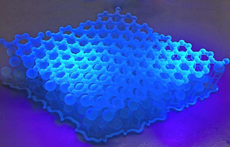
A revolutionary atom-thin semiconductor for electronics

A two-dimensional material developed by Bayreuth physicist Prof. Dr. Axel Enders together with international partners could revolutionize electronics.
Semiconductors that are as thin as an atom are no longer the stuff of science fiction. Bayreuth physicist Prof. Dr. Axel Enders, together with partners in Poland and the US, has developed a two-dimensional material that could revolutionize electronics. Thanks to its semiconductor properties, this material could be much better suited for high tech applications than graphene, the discovery of which in 2004 was celebrated worldwide as a scientific breakthrough. This new material contains carbon, boron, and nitrogen, and its chemical name is "Hexagonal Boron-Carbon-Nitrogen (h-BCN)". The new development was published in the journal ACS Nano.
"Our findings could be the starting point for a new generation of electronic transistors, circuits, and sensors that are much smaller and more bendable than the electronic elements used to date. They are likely to enable a considerable decrease in power consumption," Prof. Enders predicts, citing the CMOS technology that currently dominates the electronics industry. This technology has clear limits with regard to further miniaturization. "h-BCN is much better suited than graphene when it comes to pushing these limits," according to Enders.
Graphene is a two-dimensional lattice made up entirely of carbon atoms. It is thus just as thin as a single atom. Once scientists began investigating these structures more closely, their remarkable properties were greeted with enthusiasm across the world. Graphene is 100 to 300 times stronger than steel and is, at the same time, an excellent conductor of heat and electricity. However, electrons are able to flow through unhindered at any applied voltage such that there is no defined on-position or off-position. "For this reason, graphene is not well suited for most electronic devices. Semiconductors are required, since only they can ensure switchable on and off states," Prof. Enders explained. He had the idea of replacing individual carbon atoms in graphene with boron and nitrogen, resulting in a two-dimensional grid with the properties of a semiconductor. He has now been able to turn this idea into reality with his team of scientists at the University of Nebraska-Lincoln.
More information: Sumit Beniwal et al. Graphene-like Boron–Carbon–Nitrogen Monolayers, ACS Nano (2017). DOI: 10.1021/acsnano.6b08136
Journal information: ACS Nano
Provided by University of Bayreuth


