December 1, 2009 feature
Nanoimaging in 3-D

(PhysOrg.com) -- As technology shrinks ever smaller, interest in objects and devices on the nanoscale becomes more apparent. However, visualizing these objects in three dimensions comes with special challenges. Alexander Govyadinov, a scientist at the University of Pennsylvania, points out that imaging nano-objects in 3-D typically requires measurements of the optical phase, a task which is so difficult that it is rarely done.
Govyadinov, however, believes that there is a way around this problem by using a technique that does not require phase measurements. Govyadinov and his colleagues at the University of Pennsylvania, George Panasyuk and John Schotland, have proposed a technique that could, theoretically, provide 3 D imaging of nanostructures, without the need to measure or control phases. Their work is presented in Physical Review Letters: "Phaseless Three-Dimensional Optical Nanoimaging."
“Near-field microscopy techniques have done a great deal in terms of studying very small objects,” Govyadinov tells PhysOrg.com. “However, there are limits. One of the biggest limits is the fact that near-field techniques only allow you to see what is on the surface. You can’t go below. The object's interior, however, affects the image you obtain, such that you can get two different results when imaging the same thing using different near-field techniques.” He also points out that alternative methods for nano-imaging, such as UV and X-ray tomography, can cause damage to objects, such as occurs with degradation in nanochips, or damage to biological cells.
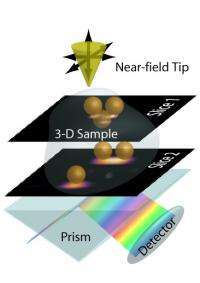
In order to get around the aforementioned problems, Govyadinov and his peers created a new technique that involves avoiding the need for phase measurements or phase-controlled illumination altogether. “As a proxy for the optical phase, we propose to employ the tip of a near-field microscope,” he explains. “This tip is a small fiber, which we can use to scan all along the surface, including up and down. By shining light on both the sample and the tip and measuring how much power is scattered away, the 3-D image can be constructed.” The purpose of the near-field tip is to modify the pattern of illumination produced inside the sample, which determines the measured power.
While it has been possible to image nanostructures in 2-D with near-field microscopes, the University of Pennsylvania team has taken it a step further in creating the capability to image nanoscale objects in three dimensions. So far, most of the applications Govyadinov sees are practical. “While there are some fundamental advantages to understanding the math, the technical applications are of more interest to us. This provides a way of imaging small things without destroying them. Moreover, it provides a chance to study beyond the surfaces of nanostructures and get an idea of what is inside.”
The next step, of course, is to move from theory to actual experimentation. "We have an experimental group very interested in our technique, and it is possible that we could see a proof of principle demonstration in a little more than a year," Govyadinov says. "If so, it would represent a big step forward in nanotechnology, and open the way for a number of useful technical applications."
More information: Alexander A. Govyadinov, George Y. Panasyuk and John C. Schotland, “Phaseless Three-Dimensional Optical Nanoimaging,” Physical Review Letters (2009). Available online: http://link.aps.org/doi/10.1103/PhysRevLett.103.213901.
• Join PhysOrg.com on Facebook!
• Follow PhysOrg.com on Twitter!
Copyright 2009 PhysOrg.com.
All rights reserved. This material may not be published, broadcast, rewritten or redistributed in whole or part without the express written permission of PhysOrg.com.


