SanDisk, Toshiba Develop 32-nanometer NAND Flash Technology
SanDisk and Toshiba today announced the co-development of multi-level cell (MLC) NAND flash memory using 32-nanometer process technology to produce a 32-gigabit (Gb) 3-bits-per-cell (X3) memory chip. The breakthrough introduction is expected to quickly bring to market advanced technologies that will enable greater capacities and reduce manufacturing costs for products ranging from memory cards to Solid State Drives (SSD).
“The development of our third-generation 3-bits-per-cell technology on 32nm within one and a half years after the introduction of the first generation of 3-bits-per-cell on 56nm shows the incredibly fast pace necessary to be a world-class producer in today’s industry,” said Sanjay Mehrotra, co-founder and president, SanDisk. “This allows us to offer higher capacities at compelling form factors while reducing manufacturing costs.”
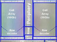
The 32Gb X3 on 32nm technology is the smallest NAND flash memory die reported so far, able to fit into the fingernail-sized microSD™ memory card format that has enjoyed widespread adoption in mobile phones and other consumer electronics devices. The 32nm 32Gb X3 is the highest density microSD memory die in the world, providing twice the capacity of a microSD chip on 43nm while still maintaining a similar die area. Advances in 32nm process technologies and in circuit design significantly contributed to a 113mm2 die-size while SanDisk’s patented All-Bit-Line (ABL) architecture has been a key enabler to maintain a competitive X3 write performance.
“The 32nm X3 die’s small footprint and incredible density will allow for the production of higher capacities of microSD cards than could be manufactured without this technology,” said Yoram Cedar, executive vice president, OEM business unit and corporate engineering, SanDisk. “The microSD form factor has grown in popularity due to rising demand for high capacity storage on mobile phones, and X3 will enable us to bring exciting new products to this market.”
32nm is the most advanced flash memory technology node to date, requiring advanced solutions to manage the challenges of feature size scaling. 32nm technology combines several innovative technologies to reduce die area more aggressively than the trend-line of Moore’s Law.
SanDisk and Toshiba today presented a joint paper on 32nm 32Gb X3 NAND flash memory at the 2009 International Solid State Circuits Conference (ISSCC), highlighting the technical advancements that made 32nm possible. Production for the 32nm 32Gb X3 is expected to begin in the second half of 2009.
Provided by Sandisk


