Philips demonstrates BAW filters for System in Package modules for wireless applications
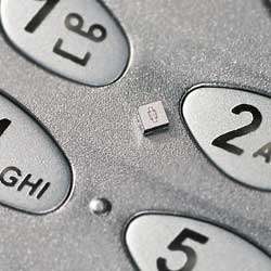
In collaboration with Philips' semiconductors division, scientists at Philips Research have developed an innovative new process technology for producing high-performance BAW (Bulk Acoustic Wave) filters on silicon wafers, each filter being housed in a chip-scale package fabricated as an integral part of the wafer processing. Aimed at replacing the SAW (Surface Acoustic Wave) and ceramic devices currently used as antenna filters in mobile phones, BAW filters fabricated in this new technology offer high performance coupled with smaller physical size. They therefore represent a critical step in reducing the footprint of RF modules so that more functionality can be squeezed into next-generation wireless products.
As more and more communications systems start to use frequency bands in the 800 MHz to 10 GHz range, antenna filters have become increasingly important in preventing one system from interfering with another system that uses close frequency bands. These filters therefore need to have bandpass characteristics that accurately match a particular system's range of carrier frequencies, together with the ability to handle the maximum RF power levels transmitted by mobiles. Compared to SAW filters, BAW filters have considerably better power handling capabilities and better temperature coefficients (typically less than 21 ppm/degree Kelvin), leading to more stable operation. Compared to ceramic filters they offer much smaller component size.
The BAW filters developed by Philips use a solidly mounted aluminum nitride BAW element to provide physical robustness and excellent power handling, mounted on a Bragg reflector to isolate acoustic vibrations from the silicon substrate. Designed using 2-dimensional modeling techniques developed specially by Philips, these BAW elements exhibit a Q-factor in excess of 1000 and a typical insertion loss of 0.5 dB per filter section (less than 2 dB total for a typical 3-section filter). A protective cover and flip-chip solder balls are added to the device during wafer processing, with devices needing no further packaging operations after the wafer is sliced up into individual components.
Philips Research has successfully demonstrated BAW resonators and filters based on this technology operating at frequencies up to 16 GHz, but believes that their main application will lie in the 800 MHz to 10 GHz ranges, serving the needs of wireless transceivers for systems such as Bluetooth, GSM/GPRS/EDGE, UMTS and IEEE 802.11a. The BAW filters can both be used as separate components and could be a part of integrated RF System-in-Package solutions for wireless applications.
Source: Philips


