October 22, 2008 feature
3D nanotube assembly technique for nanoscale electronics

(PhysOrg.com) -- For the past several years, researchers have been trying to take advantage of carbon nanotubes’ good electrical properties for future nanoscale electronics applications. One of the biggest challenges in this area is finding ways to arrange and assemble the nanotubes into 3D configurations for carrying current in nanoscale devices.
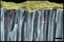
Most recently, a team of physicists and engineers from the Electronic Materials Research Institute at Northeastern University in Boston, Massachusetts, has demonstrated a technique for assembling nanotubes using an applied electric field. Using this method, the researchers could assemble single-walled carbon nanotubes into 3D structures by coaxing the nanotubes into deep nanoholes in a porous alumina template. An average of one nanotube per hole was vertically assembled, and, by sweeping the 0.32cm2 area, more than one million holes were filled with nanotubes.
“The greatest significance of this technique is that it provides the potential to manufacture, at a high rate and on a large scale, three-dimensional single-wall carbon nanotube electrical interconnects, without the need for high-temperature synthesis,” Srinivas Sridhar, Director of the Electronic Materials Research Institute, told PhysOrg.com.
To achieve this nanotube assembly, the researchers attached a positive electrode to the bottom of a silicon template, which the aluminum template went on top of. Then they manually swept a negative electrode over assembly sites, pushing negatively charged nanotubes into the holes in the aluminum template. This process of using an electric field to move charged objects is called electrophoresis. Similarly, a process called dielectrophoresis, in which a non-uniform electric field moves charged or uncharged objects, also assisted in orienting the nanotubes toward the holes.
After assembling the nanotubes, the researchers sputtered a 15-nm-thick gold layer on top of the alumina template, touching the tops of the nanotubes. This layer completed an electrical connection between all the nanotubes reaching the surface of the template, with electric current traveling through the nanotubes between the gold and silicon layers. On control samples without nanotubes, no current was observed between the two layers, confirming that the nanotubes had carried the current.
By not requiring high temperatures, and providing the ability to cover centimeter-scale areas in a short time, the new assembly technique has useful advantages over other nanotube assembly techniques. The method could also integrate well into existing silicon platforms, which could be used in microelectronics, field emission displays, electronic memory devices and solar cells.
“The next step in nanoscale electronics is to integrate the 3D carbon nanotubes architectures with current CMOS technology and create hybrid systems,” Sridhar said. “The holy grail of nanoscale electronics is to completely replace CMOS technology by monolithic carbon nanotubes devices.
“Scaling down the nominal feature size makes more space available on a chip to hold more transistors and other types of devices,” he added. “Shrinking process geometries means better performance and lower costs.”
More information: Electronic Materials Research Institute
Citation: Gultepe, Evin; Nagesha, Dattatri; Casse, Bernard Didier Frederic; Selvarasah, Selvapraba; Busnaina, Ahmed; and Sridhar, Srinivas. “Large scale 3D vertical assembly of single-wall carbon nanotubes at ambient temperatures.” Nanotechnology 19 (2008) 455309 (5pp). Contact: s.sridhar(at)neu.edu
Copyright 2008 PhysOrg.com.
All rights reserved. This material may not be published, broadcast, rewritten or redistributed in whole or part without the express written permission of PhysOrg.com.


