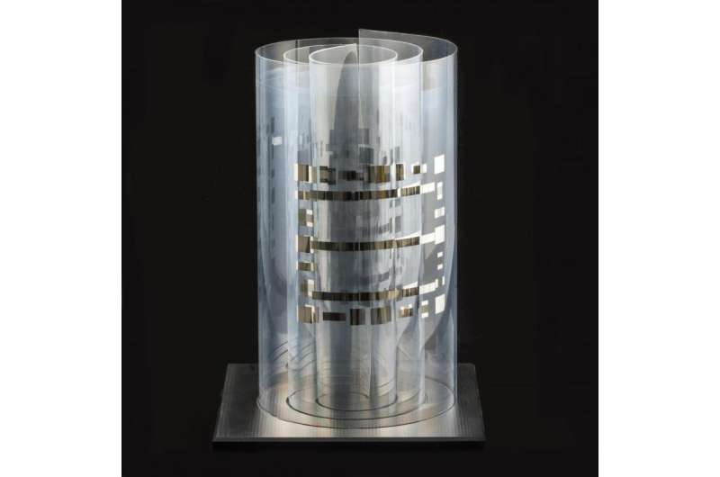
Silver circuits on foil allow curved touchscreens

Microscopically fine conductor paths are required on the surfaces of smartphone touchscreens. At the edges of the appliances, these microscopic circuit paths come together to form larger connective pads. Until now, these different conductive paths had to be manufactured in several steps in time-consuming processes. With photochemical metallization, this is now possible in one single step on flexible substrates. The process has several benefits: It is fast, flexible, variable in size, inexpensive and environmentally friendly. Additional process steps for post-treatment are not necessary.
For the new process, the foils are coated with a photoactive layer of metal oxide nanoparticles. "After that, we apply a colorless, UV-stable silver compound," Peter William de Oliveira, head of optical materials, explains. By irradiation of this sequence of layers, the silver compound disintegrates on the photoactive layer and the silver ions are reduced to form metallic, electrically conductive silver. In this way, paths of varying sizes down to the smallest size of a thousandth of a millimeter can be achieved.
This basic principle allows conductive paths to be created individually. "There are different possibilities we can use depending on the requirements: Writing conductive paths using UV lasers is particularly suitable for the initial customized prototype manufacture and testing a new design of the conductive path. However, for mass production, this method is too time-consuming," de Oliveira explains.
The researchers are currently developing a refined method using transparent stamps. "These stamps push out the silver compound mechanically; conductive paths then only occur where there is still silver compound," de Oliveira said. Since the stamps are made of a soft plastic, they can be arranged on a roll. Because they are transparent, researchers at INM are now working on embedding the UV source directly in the roll. "Thus, the initial steps for a roll-to-roll process would already have been taken," de Oliveira said. It would therefore be possible to manufacture conductive path structures of various sizes on foils on a large scale.
Provided by Leibniz Institute for New Materials


