Professor leads photonics revolution to help researchers access high-tech foundry services

(Phys.org)—Michael Hochberg joined the University of Delaware in the spring of 2012 as an associate professor in electrical and computer engineering.
An industry leader in silicon photonics and large-scale photonic-electronic integration, Hochberg is renowned for establishing Optoelectronic Systems Integration in Silicon (OpSIS), a high-tech foundry service for silicon photonics in which the community shares the cost of fabricating complex chip-scale systems across many projects.
In simplest terms, a foundry is a company or institution that builds something. One well-known example is the steel foundry, where iron ore is turned into steel beams and other items that are then shipped to different entities.
Using "shuttle runs," Hochberg says OpSIS can significantly reduce costs of building new silicon photonics devices, bringing prototyping capability for leading-edge photonics within reach of startups and academic research groups.
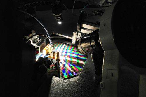
Earlier this month, OpSIS conducted its first multi-user run—creating silicon wafers approximately eight inches in diameter embedded with more than thirty unique photonics devices. This master design is replicated 30 or more times across the wafer, producing in excess of 1,000 photonics devices on each silicon substrate.
The unique devices include couplers, modulators, waveguides (optical equivalents of electrical plugs, switches, wires) and other photonic components with the potential to be attached to a fiber optics cable and used to route, control and manipulate light.
At UD, Hochberg's research team is conducting quality control testing to ensure that the optical circuits embedded in the silicon wafer perform as expected. Test structures built into the chip are used to isolate any non-performing devices to determine if fabrication error exists and to resolve problems for future production runs.
"The semiconductor industry has used the fabless manufacturing model, with specialized dedicated foundries performing the actual fabrication, for close to 50 years," explains John Wright, a researcher involved in the project. "We're taking a well-established concept and tool set and applying it to photonics."
"We are building the next wave in photonic circuits. Using a foundry service to aggregate different requests from smaller organizations, we are making it accessible to researchers, who previously wouldn't have access, to test new ideas and devices, work that may lead to future advances in photonics," continues Hochberg, who holds secondary appointments in materials science and engineering and chemical and biomolecular engineering at UD.
For UD and for researchers in the Department of Electrical and Computer Engineering in particular, this means first access to the three foundries currently working with OpSIS.
According to Dennis Prather, College of Engineering Alumni Professor, OpSIS will help revolutionize the field of silicon photonics by enabling new structures and devices to go from conceptual ideas to actual test bed systems. Having Hochberg and OpSIS at UD, he says, enables the University to become "a driving force" in this dynamic field.
"We expect to see UD develop into a center of excellence in photonics," remarks Kenneth Barner, professor and chair of the Department of Electrical and Computer Engineering.
Provided by University of Delaware


