Epson, JSR Develop World's First High-Quality Silicon Film and TFTs Using Micro-Liquid Processes

Seiko Epson Corp. and JSR have succeeded in creating the world's first high-quality silicon film with liquid coating and inkjet patterning processes. The performance of low-temperature polysilicon thin-film transistors (LTPS-TFTs) produced with silicon film formed by the spin coat method is comparable to that achieved when using silicon film formed using the conventional CVD method. The new technology is featured in the UK scientific journal Nature (April 6, 2006 issue).
With the growing demand for large displays such as liquid crystal televisions, there is an ever-increasing need for high-performance, low-cost TFTs. The existing process for manufacturing TFTs for use in displays requires enormous vacuum devices to form the film and expensive photolithography equipment to transfer the pattern, making it both costly and potentially harmful to the environment.

To address these problems, in recent years a great deal of research has been conducted on creating TFTs using organic semiconductors that can be formed from liquids. In theory, using liquid materials should not only eliminate the need for vacuum devices, but also enable the use of printing technologies such as inkjet printers to create the pattern, thereby significantly reducing energy consumption and processing time. However, the performance and reliability of existing organic TFTs are not yet sufficient for widespread use in displays. The current process makes it possible to form high-performance silicon film from liquid materials, which is the potential key to solving all of these issues at once.
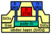
The new material jointly announced by Epson and JSR Corporation is a high order silane compound of hydrogen and silicon dissolved in an organic solvent. It forms a silicon film when spin coated on the substrate and baked in an inert atmosphere. When fabricating a TFT prototype using a silicon film formed by spin coating (other than the formation of the silicon coat, the production process is the same as for conventional LTPS TFTs), the electrons achieved mobility of 108 cm2/Vs. The new material shows high potential, as this is approximately the same mobility achieved using the CVD method.
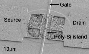
Epson used its proprietary "micro liquid processes" to demonstrate the possibilities of printed TFTs, forming a silicon film pattern onto a substrate by firing the materials onto a substrate using the inkjet method. As a result, part of the pattern formation associated with traditional photolithography is unnecessary. Forming a TFT prototype using a silicon film pattern using the inkjet method (other than the formation of the silicon coat pattern, the production process is the same as for conventional LTPS TFTs) the electrons achieved mobility of 6.5 cm2/Vs, a figure that is lower than that achieved with spin coating. Although improvements need to be made to the inkjet process, Epson believes that printed TFTs show sufficient potential.
This research was commissioned by Japan's New Energy and Industrial Technology Development Organization (NEDO), an incorporated administrative agency, as a project entitled, "Development of Manufacturing Technology for Silicon Transistors Using Liquid Materials", with the aim of advancing research on fundamental technology.
Source: Seiko Epson


