Fujitsu: World's First Technologies to Form and Multi-layer High Dielectric Constant Ceramic Film on Resin Circuit Board
Fujitsu Limited and Fujitsu Laboratories Ltd., in collaboration with the National Institute of Advanced Industrial Science and Technology (AIST) of Japan, today announced that they have jointly developed the world's first technologies that enable the formation and multi-layering at room temperature of ceramic film with dielectric constant(1) of 400, on resin circuit boards. The new technologies makes it possible to embed passive components such as condensers into printed circuit boards, such as FR4(2), thereby achieving miniaturization and cost reductions of circuit boards.
The technologies were developed as part of basic research to realize further miniaturization of devices for the ubiquitous networking era, by integrating resin with ceramic materials. Details of the new technology will be presented at the International Conference on Crystal Growth (ICCG) to be held from August 9 in Grenoble, France. Research for the new technology was commissioned by the New Energy and Industrial Technology Development Organization (NEDO), as part of the Nano Structure Forming for Advanced Ceramic Integration Technology Project, a nano-technology program of Japan’s Ministry of Economy, Trade, and Industry.
Background
In ubiquitous networking, multi-functionality, miniaturization, high-speed transmissions, and cost reduction of electronic devices are considered to be key and necessary factors. To meet these needs, currently there is much interest in technology for high-density mounting. For example, multi-functions such as GPS and wireless LAN are increasingly being included in mobile devices, resulting in larger circuit boards. To achieve miniaturization of these devices, it is necessary to reduce and integrate various high-frequency components, such as ceramic chip condensers, on the surface of circuit boards.
Embedding ceramic condensers with high dielectric constant into printed circuit boards made mainly with low-cost epoxy resin, widely used in the market now, enables further multi-functionality, miniaturization, and cost reduction of electronic devices.
Technological Challenges
Since the endurance temperature of epoxy-based resin circuit boards is approximately 300 degrees Celsius, it was fundamentally impossible in the past to embed ceramic condensers that require high temperatures for formation, into circuit boards. Another method exists in which a composite material consisting of ceramic dispersed into resin is used. However, as the dielectric constant of this method is low at only several ten, this method was unable to meet performance requirements for high frequencies.
Technology in which the circuit board itself is created with ceramics requires high temperatures of approximately 1000 degrees Celsius, thus necessitating complicated processes and making cost reductions difficult. Furthermore, volume shrinkage of over 10 percent which occurs during the manufacturing process hinders achieving accurate dimensions, resulting in inabilities to fulfill miniaturization demands.
Newly Developed Technologies
Fujitsu and the National Institute of Advanced Industrial Science and Technology (AIST) of Japan jointly developed two new technologies: a technology that forms at low temperatures ceramic film with high dielectric constant on resin circuit boards, and a technology that enables multi-layering of condenser structures. Features of these new technologies are follows:
1. Technology to create ceramic film on resin circuit boards at low temperatures
This technology enables the creation of ceramic film on resin circuit boards at room temperature, by utilizing the aerosol deposition method. In the aerosol deposition method, gas flow is used to carry ceramic powder, which is sprayed at high speeds onto circuit boards, thereby creating a ceramic film resulting from the impact. By utilizing ceramic particles that feature chemically unstable surface characteristics, ceramic film was successfully created at room temperature on resin circuit boards which ceramic is usually difficult to adhere to. This technology was jointly developed with Dr. Jun Akedo and his group at the Advanced Manufacturing Research Institute of the National Institute of Advanced Industrial Science and Technology, the same group that developed the aerosol deposition method.
2. Technology to enable high dielectric constant and multi-layering of ceramic film
High dielectric constant was achieved by mixing in highly crystalline ceramic particles, and controlling the nano-structure of the ceramic to be formed by optimizing the flow speed of the ceramic particles. A multi-layer condenser was successfully created on a resin circuit board by relaxing internal stress(3) within the ceramic film that was created, and by selecting an electrode that is composed of metal and easily adheres to ceramic film.
Results
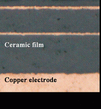
By utilizing the new technologies, the world's first ceramic film formed at room temperature on an FR4 printed circuit board was successfully created (Figures 1 and 2). The maximum dielectric constant of the newly created ceramic film was 400, ten times the dielectric constant of ceramic combined with resin, and is approximately at the same level as that of ceramic film made with the sputtering method that employs heat-treating at the high temperature of 600 degrees Celsius. A condenser composed of three layers was also successfully created on an FR4 printed circuit board. The capacitance density(4) of the newly created condenser achieved 300 nano-farad/cm2, a high level that is ideal for practical use.
The new technologies contribute significantly to further multi-functionality, miniaturization, high-speed transmission, and cost reduction of various products for the ubiquitous networking era. Potential product applications include:
Printed circuit boards and packaging with embedded condensers
Modules integrating various ceramic microwave components (filters, antennas, etc.)
Microwave electronic components
Future Developments
In addition to developing creation of ceramic dielectric at low temperatures to target higher dielectric constant, Fujitsu will promote research and development of ceramic film that has characteristics ideal for a variety of device applications, and continue development to aim for the practical use of condensers embedded in printed circuit boards.
Glossary and Notes
(1) dielectric constant: An index representing the degree to which substances can store electric charge. The higher the value is the more electric charge can be stored, thereby indicating that a substance is superior as a condenser material.
(2) FR4: Flame Retardant Type 4. The name of a flame retardant printed circuit board composed compositely of glass fibers and epoxy resin.
(3) internal stress: Stress buildup within a material resulting from strain due to mechanical or thermal factors.
(4) capacitance density: A value expressing the stored electrical charge within unit areas of components such as condensers. The higher this value is the more efficiently electric charge can be stored.
Source: Fujitsu Limited


