Freeze casting—a guide to creating hierarchically structured materials
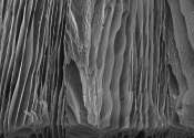
Freeze casting is an elegant, cost-effective manufacturing technique to produce highly porous materials with custom-designed hierarchical architectures, well-defined pore orientation, and multifunctional surface structures. ...


