Finding the True Measure of Nanoscale 'Roughness'
Straight edges, good. Wavy edges, bad. This simple description holds true whether you are painting the living room or manufacturing nanoscale circuit features.
In a technical paper* published in June, researchers at the National Institute of Standards and Technology (NIST) and SEMATECH describe an improved method for determining nanoscale "linewidth roughness," an important quality control factor in semiconductor fabrication. Their research shows that current industry measurement methods may be exaggerating roughness of the smoothest circuit features by 40 percent or more above true values.
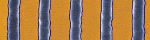
Image: A colorized scanning electron microscope image shows the "waviness" or roughness of edges on reference lines made of silicon that are about 100 nanometers wide. Credit: B. Bunday, SEMATECH/K. Talbott, NIST
As circuit features shrink in size to below 50 nanometers, wavy or rough edges within semiconductor transistors may cause circuit current losses or may prevent the devices from reliably turning on and off with the same amount of voltage.
"With this type of measurement," says NIST's John Villarrubia, "besides the real roughness there is also a false roughness caused by measurement noise. Our method includes a correction to remove bias or systematic error from the measurement."
Random noise, by definition, causes the measured value to be sometimes higher, sometimes lower than the true value, and can be minimized by simply averaging an adequate number of measurements. Systematic error, however, is consistently above or consistently below the true value due to some quirk of the measurement method.
The noise in nanoscale scanning electron microscope (SEM) images consistently adds extra roughness, says Villarrubia. The NIST/SEMATECH method involves taking two or more images at exactly the same location on a circuit feature, comparing the values, and subtracting the false roughness caused by measurement noise. SEM manufacturers should be able to incorporate the new method into their proprietary software for automated linewidth roughness measurements.
* J.S. Villarrubia and B.D. Bunday, Unbiased Estimation of Linewidth Roughness, Proceedings of SPIE 5752 (2005) pp. 480-488.
Source: NIST


