Casio and Renesas Technology to Collaborate on Semiconductor Device Packaging Technology
Casio Computer Co., Ltd. and Renesas Technology Corp. have agreed to an arrangement whereby Casio will license its wafer level package (WLP) semiconductor device packaging technology to Renesas Technology.
The agreement marks the first time Casio has made its WLP technology available to another Japanese semiconductor device manufacturer.
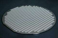
Image: Wafer Level Package (Flash Memory) Wafer
The main points of the agreement are:
1. Casio will make its WLP technology available to Renesas Technology on an ongoing basis. Renesas Technology will make active use of WLP in the fabrication of its semiconductor devices.
2. Renesas Technology will be authorized to manufacture and sell chip size package (CSP)*1 products employing WLP, both on its own and through its subsidiaries.
WLP is a new technology for semiconductor devices that enables rerouting of the copper traces and encapsulation of the chips in epoxy resin while the wafer is intact. There is an increasing demand for electronic products that are more compact and offer a high level of performance, and WLP technology is ideal for applications such as mobile phones and digital cameras. Casio's group company CASIO Micronics is already using Renesas Technology semiconductor devices that have been processed using WLP in its products.
Renesas Technology also has an in-house developed wafer process package (WPP) technology. Like WLP, it enables rerouting of the copper traces while in the wafer stage and is used in the manufacture of CSP devices. The license agreement with Casio will enable Renesas Technology to better meet the requirements of its customers by offering a broader array of package options.
Both Casio and Renesas Technology anticipate that the present agreement will lead to an even stronger relationship between the two companies in future.
Notes:
1. Chip Size Package (CSP): CSP is a semiconductor package that has roughly the same external dimensions as the bare chip. Such packages are used in all sorts of compact and lightweight electronic products. Mobile phones are a typical example.


