April 11, 2023 feature
This article has been reviewed according to Science X's editorial process and policies. Editors have highlighted the following attributes while ensuring the content's credibility:
fact-checked
peer-reviewed publication
trusted source
proofread
Prolonged photostability in hexagonal boron nitride quantum emitters
Single-photon emitters are crucial building materials suited for optical quantum technologies. Among them, hexagonal boron nitride is a promising two-dimensional material that retains bright, room-temperature single-photon emitters. However, photo-instability is an existing challenge to facilitate applications of these properties in practice.
In a new study published in Communications Materials, Sylvia Xin Li and a team of scientists at the department of Chemical Engineering, Massachusetts Institute of Technology, University of Texas, RIKEN center for Advanced Photonics, and the University of Oxford, revealed the possibility of photobleaching hexagonal boron nitride vacancy emitters to facilitate photostability suited for quantum applications.
Designing quantum emitters
Quantum mechanics can be harnessed for real-world applications as one of the most intriguing and fastest growing technologies exploring quantum states of photons for information processing and transmission. Researchers have investigated a variety of solid-state single photon sources in three-dimensional crystals; however, the light emanating from these sources can be contained by the surrounding bulky dielectric environment to cause reduced efficiency of emission.
Scientists can overcome this challenge of color centers in two-dimensional hosts such as transition metal dichalcogenides and hexagonal boron nitrides (hBN) via dielectric materials with significantly reduced thickness at the level of a single atomic layer to integrate with on-chip photonics. While single photon emission in transition metal dichalcogenides is only observed at room temperature, the material itself can host bright, room-temperature single-photon emitters to provide materials such as hexagonal boron nitride with unique photophysical properties to function at cryogenic temperatures.
Atomic-scale imaging
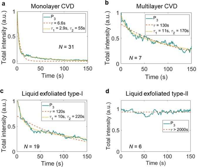
In this work, Li and colleagues quantitatively studied the photobleaching lifetimes of various hexagonal boron nitride samples and revealed them to be dominated via photochemical reactions with oxygen. The team showed bleaching to be significantly reduced by a simple strategy of stacking additional monolayers of the compound on the material.
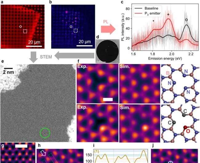
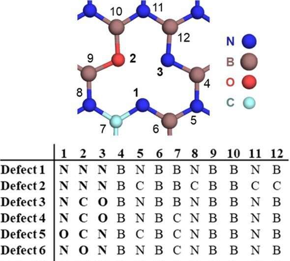
The scientists characterized the photobleached monolayer with annular dark-field scanning transmission electron microscopy to achieve high-quality atomic scale imaging of the hBN lattice. They combined X-ray photoelectron spectroscopy and annular dark-field scanning transmission electron microscopy to achieve high-quality atomic-scale imaging of the hexagonal boron nitride lattice.
The photostability of emitters in various hexagon boron nitride (hBN) samples
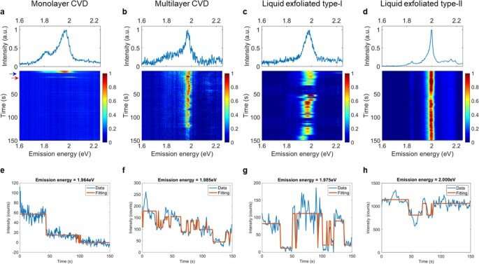
The research team compared three commercially available hBN thin films, including monolayer chemical vapor deposition grown hexagon boron nitride on copper foil, multilayer chemical vapor deposition grown hBN on copper foil and multilayer-liquid-exfoliated hBN nanoflakes suspended in ethanol/water mixtures. The team transferred these samples into silicon dioxide substrates without any post-treatment and examined them with time-dependent photoluminescence measurements by using a custom-built confocal spectroscopic microscope.
Li and colleagues focused on the emitter species observed in all hBN samples and noted the presence of three different emission behaviors in monolayer and multilayer chemical vapor deposition samples. Multilayer liquid exfoliated hexagonal boron nitride as-prepared without thermal annealing treatment showed two different emission modes of interest, which they characterized extensively.
Bleaching mechanisms in monolayer chemical vapor deposition hexagonal boron nitride (hBN)
The scientists studied the bleaching mechanisms of monolayer hBN emitters under a variety of atmospheres using a custom-built environmental chamber. They accomplished this by placing a monolayer sample of chemical vapor-deposition grown hexagonal boron nitride in a small sealed chamber with a quartz observation window and filled the gas chamber with a variety of gases, including nitrogen, oxygen and water vapor. Since many organic fluorophores are degraded with oxygen or water, the team filled the environmental chamber with nitrogen to minimize hydration.
While the nitrogen atmosphere did not mitigate bleaching completely when the team conducted bleaching experiments in an oxygen-rich atmosphere, they noted its influence in the process of photobleaching. The scientists further examined bleaching mechanisms of the material via annular dark-field in the scanning transmission electron microscope (ADF-STEM).
Chemical analysis and thermal annealing effects
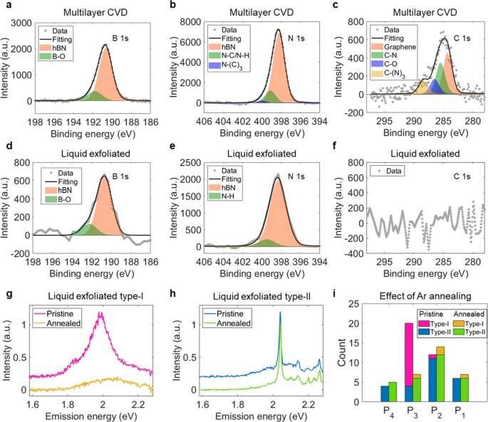
Li and colleagues conducted X-ray photon spectroscopy to identify different elements and their chemical states with the materials in contrast to elemental analysis with inductively coupled plasma techniques. To accomplish this, they first sputtered the sample surfaces with an argon ion beam to remove any adsorbed hydrocarbons. As the timeframe of Argon sputtering increased, the atomic concentration of carbon on the multilayer surface decreased to reach a stable value. The outcomes were consistent with ADF-STEM imaging outcomes of the monolayer compound.
With higher surface carbon concentrations, the researchers grew atomic layers of hybridized boron nitride and graphene domains with methane and ammonia borane as precursors. They then synthesized hBN from a lab-built, low-pressure chemical vapor deposition reactor with typical hBN crystals of triangular shape, and observed the materials with scanning electron microscopy. The team also noted the presence of polygonal sheets in similar regions, which they credited to the presence of graphene by analyzing the regions with Raman spectroscopy.
Outlook
In this way, Sylvia Xin Li and a research team in engineering, chemistry and photonics, identified a key to improve the photostability of emitters in hexagonal boron nitride materials that effectively shielded oxygen from the environment to optimize carbon substitution in the hexagonal boron nitride (hBN) lattice. They noted photobleaching of hBN emitters to be in direct contact with air, and dominated by photochemical reactions emitting defects with oxygen. The team mitigated the effects of bleaching by shielding molecular oxygen and by introducing a nitrogen atmosphere, or by stacking additional hexagonal boron nitride layers on the material.
This strategy improved the average emitter lifetime by about 20 times. The team compared the experimental results across a range of imaging methods and thermal annealing to verify the outcomes to provide in-depth insights to the structural origins of hBN quantum emission. The knowledge gained about defect engineering hexagonal boron nitride will be insightful across broader fields of study to tune the electric properties of materials within 2D integrated devices and in 2D quantum materials for future sensing.
More information: Sylvia Xin Li et al, Prolonged photostability in hexagonal boron nitride quantum emitters, Communications Materials (2023). DOI: 10.1038/s43246-023-00345-8
Toan Trong Tran et al, Quantum emission from hexagonal boron nitride monolayers, Nature Nanotechnology (2015). DOI: 10.1038/nnano.2015.242
Journal information: Nature Nanotechnology
© 2023 Science X Network


