This article has been reviewed according to Science X's editorial process and policies. Editors have highlighted the following attributes while ensuring the content's credibility:
fact-checked
peer-reviewed publication
trusted source
proofread
Tailoring thickness of conducting materials to enhance their photonic applications

Purdue University researchers found that by tailoring the film thickness of conducting nitrides and oxides, specifically plasmonic titanium nitride (TiN) and aluminum-doped zinc oxide (AZO), they can control the materials' optical properties, most notably their epsilon near zero (ENZ) behaviors. The TiN and AZO materials developed at Purdue also feature the lowest reported optical losses. This provides novel applications for the telecommunications field and furthers the study of many optical nonlinearities.
Vladimir M. Shalaev and Alexandra Boltasseva, Purdue professors of electrical and computer engineering, and their team of researchers, led by then-postdoctoral researcher Soham Saha, investigated this method of controlling the ENZ point, the wavelength at which a material is neither dielectric nor metallic.
When light travels through an ENZ material, its group velocity slows to near zero, and it's able to interact with the material for a longer period. This gives rise to many interesting nonlinearities. However, with most conventional materials, the ENZ point is fixed and difficult to move.
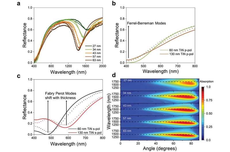
What the researchers demonstrated is that the thickness association of the optical properties is one of the easiest things to manipulate, enabling them to grow films with different ENZ properties using the same growth environment. By tailoring the thickness of material films and controlling light absorption near the ENZ regime, researchers can study absolute ENZ physics at many different wavelength ranges. The enables a wide range of nonlinear optical phenomena, including all-optical switching, time refraction and high-harmonic generation.
In their study, the researchers developed a low-loss, polycrystalline films of TiN on silicon by reactive magnetron sputtering. AZO was grown by pulsed laser deposition on the as-grown TiN. They investigated the cause of the thickness-dependent optical properties through spectroscopic ellipsometry, atomic force microscopy and transmission electron microscopy, connecting the optical properties to their structural properties.
As a proof of concept of a dynamic, tunable device, researchers demonstrated all-optical switching of the resonators using an interband pump, showing picosecond relaxation times.
The study is published in the journal Advanced Materials.
More information: Soham Saha et al, Tailoring the Thickness‐Dependent Optical Properties of Conducting Nitrides and Oxides for Epsilon‐Near‐Zero‐Enhanced Photonic Applications, Advanced Materials (2022). DOI: 10.1002/adma.202109546
Journal information: Advanced Materials
Provided by Purdue University


