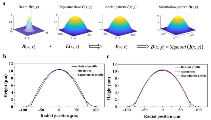
a, In this imaging example, B(x, y) is the gaussian beam, E(x, y) is the exposure dose sampled by structure. The aerial pattern I(x, y) convolving B(x, y) and E(x, y). Finally, the resist effect is described by the differentiable sigmoid function, and the simulation pattern D(x, y) is approximated by Sigmoid (I(x, y)). b-c) Schematic illustration of the AMLA profile b, before and (c) after OPC, where black, red and blue lines represent target profile, simulation profile and experimental profile of AMLA respectively. Credit: Shiyi Luan, Fei Peng,Guoxing Zheng, Chengqun Gui, Yi Song, and Sheng Liu
As a structure composed of two-dimensional arrays of microscale lenses, micro-lens array (MLA) has attracted the attention of both academia and industry due to its distinctive optical properties and wide applications. Recently, MLA has gradually stepped into diverse application fields, such as wave front sensing, virtual reality/augmented reality display, beam shaping, micro/wide viewing angle imaging, light-field camera, optical communication and many other emerging applications.
However, with the traditional MLA fabrication approaches, such as the hot reflow, ink-jet and self-assembly, it is difficult to fabricate aspheric micro-lens array (AMLA) directly with a desired arrangement and profile, which determines AMLA's optical performances. Meanwhile, the drawbacks, such as the debris induced by the top-down writing, difficulties in the topography controlling and the process complexity, hinder these methods from large-scale commercialization.
In a new paper published in Light: Advanced Manufacturing, a team of scientists, led by Professor Chengqun Gui from State Key Laboratory of Advanced Lithography, The Institute of Technological Sciences, Wuhan University, Wuhan, and co-workers have demonstrated the fabrication and characterization of AMLA via the single beam exposure DLWL, which can satisfy the high requirement of optical performances.
To control the profile, an optimization method was employed in our study to reduce the AMLA profile deviation from the desired one. Parallel and scattered light sources were used to test the different optical performances of the AMLA, and the results meet quite well with our design. Due to the high flexibility of our approach, AMLA with different filling factors and an off-axis AMLA can also be readily fabricated with the one-step photolithography. Finally, an auto-stereoscopic-display with flexible thin film has been prepared by using above technology, which exhibits a new way to provide flexible holographic display at low cost.
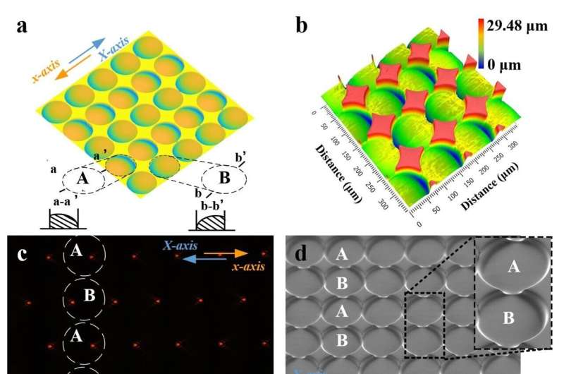
a, Schematic diagram of an off-axis MLA. b, Three-dimensional topography of a fabricated off-axis MLA. c, Experimentally captured focused spot arrays with the operating wavelength of 635 nm. d, Off-axis MLA characterized via the SEM. e-f, SEM photos in partial views of the MLAs with filling factors of 90.7% and 100%. Credit: Shiyi Luan, Fei Peng,Guoxing Zheng, Chengqun Gui, Yi Song, and Sheng Liu
Compared to the traditional MLA fabrication methods, this advanced photolithography technology is the high flexibility in design, which can significantly improve the performance of many functional devices based on MLA. These scientists summarize the advantage and application prospect of this advanced photolithography technology:
"We show the AMLA with dimensions of 30 × 30 mm2 can be fabricated within 8 h 36 min, corresponding to a high-speed writing exceeding 100 mm2/h. In fact, we can fabricate MLA with area larger than 500× 500 mm2.Meanwhile, the profile of fabricated AMLA was optimized successfully via a three-dimensional optical proximity correction (relative profile deviation down to 0.28%) and surface roughness was sub 6 nm in average."
"It has many application prospects, such as laser beam shaper and wave-front sensor. For example, to realize a freeform beam shaper, the micro-lenses inside a MLA should be aligned irregularly (i.e., the focused spot arrays are randomly distributed), which requires a complex greyscale mask for other approaches. Using the laser direct writing lithography technology with a high degree of manufacturing freedom, we can directly fabricate an off-axis MLA to generate unregular spot arrays without the requirement of a complex greyscale mask," they added.
"The proposed AMLA fabrication method based on the direct laser writing lithography can not only reduce the difficulty of preparing complex morphology MLAs, but also be very suitable for industrial production. This may greatly reduce the preparation cost of devices composed of micro-lens, such as endoscopes, infrared detectors, holographic displays, optical couplers, etc. Therefore, it would have big impact on the medical treatment, rescue, optical communication, military and many other related fields," the scientists said.
More information: Shiyi Luan et al, High-speed, large-area and high-precision fabrication of aspheric micro-lens array based on 12-bit direct laser writing lithography, Light: Advanced Manufacturing (2022). DOI: 10.37188/lam.2022.047
Provided by Chinese Academy of Sciences


