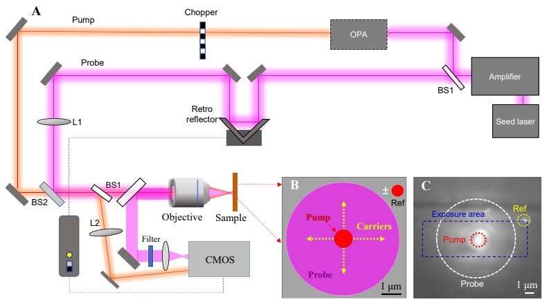
Setup of transient reflectivity mapping system. (A) Schematic illustration of the transient reflection mapping apparatus. (B)Schematic illustration of the wide field detection. (C) Pulses intensity distribution on the surface of sample 2. The pump beam was focused onto the surface (within a red dotted circle) while probe beam was de-focused to create the wide field detection, marked by a white circle. The exposure area is marked by a blue rectangle, a reference beam (yellow dotted circle) was focused onto the target surface of the camera directly, In the actual measurement, the pump beam was blocked by a long pass filter. Credit: Science (2022). DOI: 10.1126/science.abn4727
Cubic boron arsenide (c-BAs), a semiconductor with ultrahigh thermal conductivity comparable to diamond, has attracted wide attention since 2018, with many people wondering whether it is suitable for transistors.
Researchers trying to answer this question measured the Hall effect for a single crystal of c-BAs in 2021, obtaining the disappointingly low mobility figure of 22 cm2V-1s-1. In addition, their results showed a huge discrepancy between the theoretical mobility value of 1400 cm2V-1s-1 for electrons and 2110 cm2V-1s-1 for holes.
In a study published in Science, Liu Xinfeng's group from the National Center for Nanoscience and Technology (NCNST) of the Chinese Academy of Sciences (CAS) and collaborators from the University of Houston have now obtained accurate mobility figures for c-BAs. They found that the ambipolar mobility of c-BAs is about 1550 cm2V-1s-1 and more than 3000 cm2V-1s-1 for hot carriers with much higher mobility.
The researchers used a distinctive optical technique called transient reflectivity microscopy to monitor carrier diffusion in c-BAs.
This technical setup, built by Yue Shuai from Liu's group, provides in-situ carrier diffusion visualization with spatiotemporal resolution in nanometers and femtoseconds. Carriers were excited by a femtosecond laser, which created a transient reflectivity change that was detected by a time-delayed femtosecond laser (probe beam).
The probe beam was broadened to a wide illumination field; thus, the carriers' spatiotemporal dynamics could be visualized directly. By adjusting the energy of the excitation laser below or above the bandgap, intrinsic carriers and hot carriers could be excited, respectively. Intrinsic carrier mobility of about 1550 cm2V-1s-1 was measured and matched theoretical predictions well.
Due to ultraweak electron-phonon and phonon-phonon coupling, a long-lasting hot carrier with mobility greater than 3000 cm2V-1s-1 was further obtained.
The researchers said that the huge difference between the Hall effect measurement and the optical measurement was due to the wide distribution of defects in the sample. In other words, only a small region was pure enough for carrier diffusion.
"After a year's hard work, we finally found the region," said Yue, first author of the paper. "It was too small for the Hall measurement."
Liu said the high mobility and ultrahigh thermal conductivity of c-BAs makes it a "promising material" in the wide field of electrical circuits and will help to improve CPU speeds.
More information: Shuai Yue et al, High ambipolar mobility in cubic boron arsenide revealed by transient reflectivity microscopy, Science (2022). DOI: 10.1126/science.abn4727
Journal information: Science
Provided by Chinese Academy of Sciences


