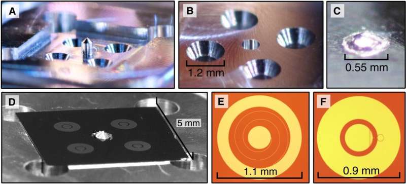
Optical images of cavity enclosure and circuit. (A) Enclosure base with cavity, central pillar, and four tapered through-holes for out-of-plane wiring access. (B) Enclosure lid with a central cylindrical recess and identical through-holes for out-of-plane wiring. (C) Cylindrical recess in the lid filled with a ball of indium. (D) (Grayscale) Four-qubit circuit mounted inside the enclosure base. The four qubits are visible, arranged in a square lattice with 2-mm spacing. (E) A spiral resonator and (F) a transmon qubit with identical electrode dimensions to those in the device. Credit: Science Advances (2022). DOI: 10.1126/sciadv.abl6698
In a new report now published in Science Advances, Peter A. Spring and a team of scientists in physics at the Oxford University described qubit coherence and low cross-talk and single-qubit gate errors in superconducting qubit architecture, suited for two-dimensional (2D) lattices of qubits. The experimental setup involved an inductively shunted cavity enclosure with non-galvanic, out-of-plane control wiring, qubits and resonators fabricated on opposing sides of a substrate. The scientists developed a proof-of-concept device featuring four uncoupled transmon qubits, i.e., a superconducting charged qubit with reduced sensitivity to charge noise, to exhibit specific features measured via simultaneous randomized benchmarking. The three-dimensional integrated nature of the control wiring allowed the qubit to remain addressable as the architecture formed larger qubit lattices.
Quantum architect
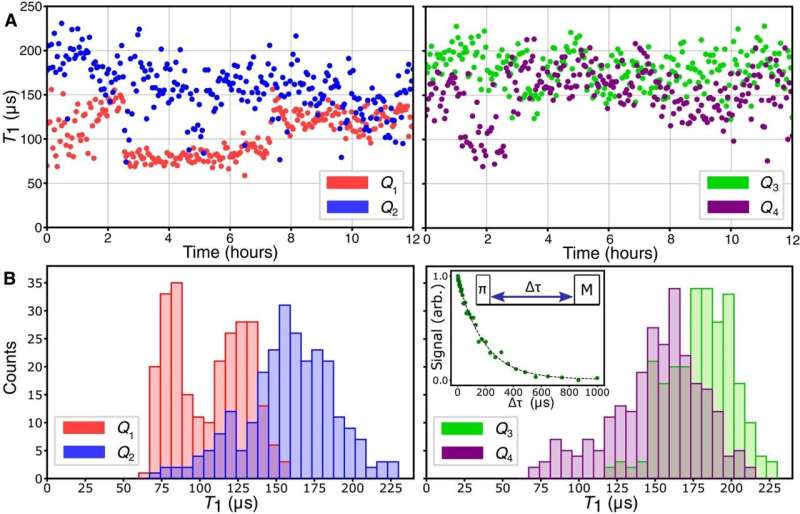
Efforts to build three dimensional (3D) lattices with multitudes of highly coherent qubits enclosed is an outstanding hardware challenge. Researchers have previously developed superconducting circuits as a promising platform to realize such lattices and form a universal gate set. Typically, two sets of requirements must be met to scale such superconducting lattices, including a method to route control wiring to the circuit allowing all qubits to remain addressable and measurable, while preventing low frequency spurious modes from emerging within the circuit with increasing dimensions. The scaling process should also prevent decoherence channels to qubits and be compatible with gate fidelities beyond the threshold of quantum error correction codes. Physicists had previously overcome wiring limits of edge connected circuits via 3D integrated control wiring as a practical solution. Alternatively, circuits can be enclosed in inductively shunted cavities in two dimensions with a cutoff frequency to cavity modes. Spring et al presented experimental results relative to the latter concept on a four-qubit proof-of-principle circuit, where the circuit architecture featured 3D integrated out-of-plane control wiring, qubits and readout resonators fabricated on opposing sides of a substrate. The team also included a key new feature for compatibility with transmon coherence times, exceeding 100 µs, low cross-talk and single-qubit gate errors.
-
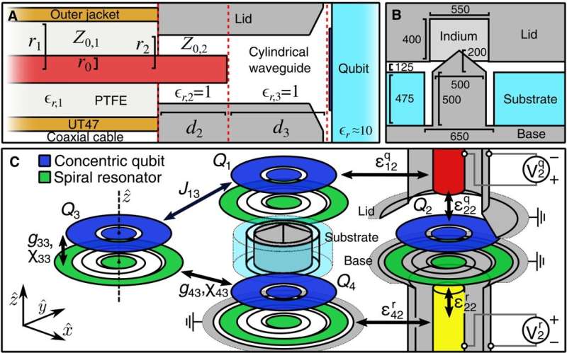
Device schematics. (A) Cross section of the out-of-plane wiring design (not to scale), here shown addressing a qubit. PTFE, polytetrafluoroethylene. (B) Cross section of the bulk via inductive shunt design (to scale). The designed dimensions are shown in micrometers. (C) Circuit layout illustration (not to scale). The substrate and enclosure are partially shown, and the out-of-plane wiring is shown for Q2. Examples of the coupling terms and drive voltages in the Hamiltonian. Credit: Science Advances (2022). DOI: 10.1126/sciadv.abl6698
-
Qubit relaxation characterization. (A) Two hundred fifty-one consecutive T1 measurements over an approximately 12-hour period. (B) Resultant histograms of T1. The inset shows an example T1 time trace for Q3, and the measurement pulse sequence. The four qubits were measured simultaneously; the data are shown across two graphs for legibility. Credit: Science Advances (2022). DOI: 10.1126/sciadv.abl6698
Device architecture and cross-talk characterization
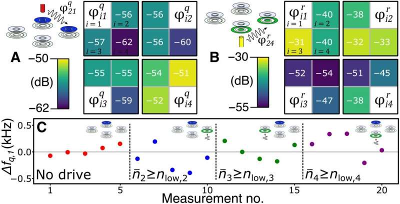
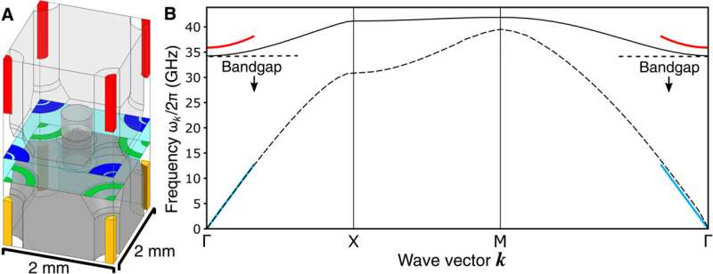
The researchers obtained images of the cavity enclosure and circuit, where the enclosure base maintained a single central "pillar" and a lid containing a matching cylindrical recess filled with a ball of indium. They arranged the four coaxial transmon qubits in a 2 x 2 lattice with 2 mm spacing and then implemented an out-of-plane wiring design with inductive shunt design, and a circuit layout, where each resonator was coaxially aligned with, and capacitively coupled, to a qubit. The setup allowed the qubit electrodes to be "electrically floating." The team obtained the basic circuit parameters and characterized cross-talk of the device, where the device was a proof-of-principle demonstration of the circuit architecture without intentional couplings, except between qubit-resonator pairs. As a result, Spring et al identified all other couplings as undesired cross-talk. The team then defined the terms of cross-talk and summarized the experimental and simulated parasitic transverse couplings in the device followed by experimental measurements of qubit control line selectivity, and resonator control line selectivity. They also measured the parasitic qubit-resonator coupling to understand the parasitic dispersive shift between qubit and resonator. Followed by single-qubit randomized benchmarking performed on all four qubits separately and simultaneously. The team conducted each of the 31 x 80 experiments, 5,000 times to build statistics and presented the resulting error-per-physical gates, and also performed correlated randomized benchmarking based on simultaneous experimental data. For band structure simulations, Spring et al analyzed the high-frequency structure simulator model of a unit cell that contained ideal dimensions of the central 2 mm x 2 mm, region of the device. They then mapped the band structure during simulations while gathering details on the analytical cutoff frequency, band curvature, and plasma skin and depth predictions within the setup.
-
Cross-talk characterization. (A) Experimentally measured qubit control line selectivity φqij=(εqij/εqjj)2 from qubit i to qubit control line j, expressed in units of dB as 10log10(φqij) . (B) Experimentally measured resonator control line selectivity φrij=(εrij/εrjj)2 from resonator i to resonator control line j, expressed in units of dB as 10log10(φrij) . (C) Frequency variation in Q1 found from 20 repeated Ramsey experiments, with either no drive on any resonator or a continuous drive applied to R2, R3, or R4 at frequency ωr, j that populates it with a photon number n¯j of at least nlow, j ≝ ncrit, j/10. Credit: Science Advances (2022). DOI: 10.1126/sciadv.abl6698
-
. Band structure simulation. (A) HFSS model of a unit cell featuring a single addressable and measurable qubit (4 × 1/4) and a single pillar that inductively shunts the enclosure. The unit cell has identical dimensions to the 2 mm by 2 mm central region of the device measured in this work. (B) Simulated lowest-band dispersion for the infinite enclosure formed by tiling the plane with the unit cell, with (solid) and without (dashed) the inductively shunting pillar and associated substrate aperture. The wave vector k traces between the symmetry points Γ : (kx = 0, ky = 0), X : (kx = π/a, ky = 0), M : (kx = π/a, ky = π/a). The colored curves show the predicted curvature around the Γ point with (red) and without (blue) the inductively shunting pillar and associated substrate aperture, using no free fit parameters. Credit: Science Advances (2022). DOI: 10.1126/sciadv.abl6698
Outlook
In this way, Peter A. Spring and colleagues analyzed average qubit coherence times and simultaneous single-qubit gate fidelities in a four-qubit demonstration of a 3D superconducting circuit architecture. Prior to qubit coupling circuitry inclusion, the team highly suppressed the residual crosstalk of the setup. The envisioned optimized device is applicable to study correlated errors generated from high energy radiation in lattices of qubits with high coherence and exponentially suppressed cross-talk. The present architecture contained an inductively shunted cavity enclosure tightly surrounding the circuit, combined with 3D integrated out-of-plane control wiring and reverse-side readout resonators. The outcomes highlighted the low cross-talk of the experimental setup. The enclosure package is reusable by reshaping the indium ball in the lid recess; however, the circuit was not bonded to the enclosure and could not be removed and remounted therefore. The scientists highlighted several shortcoming of the presented device, including the small and variable external resonator-decay rates and dispersive shifts that were non-optimal for qubit readouts. Spring et al. credited the increased coherence in the setup to the fabrication process, which differed from previous implementations of the architecture.
More information: Peter A. Spring et al, High coherence and low cross-talk in a tileable 3D integrated superconducting circuit architecture, Science Advances (2022). DOI: 10.1126/sciadv.abl6698
G. Fowler et al, Surface codes: Towards practical large-scale quantum computation, Physical Review A (2012). DOI: 10.1103/PhysRevA.86.032324
Journal information: Physical Review A , Science Advances
© 2022 Science X Network
