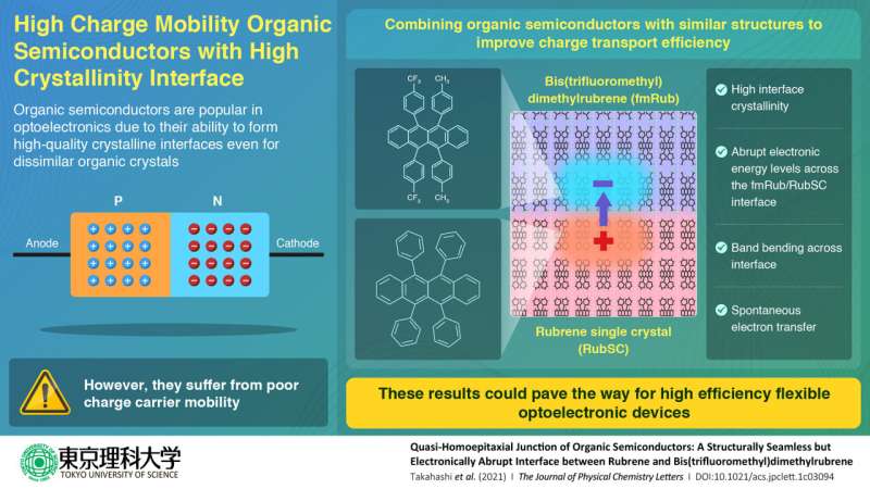
Organic molecular interfaces with minimized structural mismatch and spontaneous electron transfer could open doors to high-efficiency optoelectronics. Credit: Tokyo University of Science
Semiconductor electronic devices can be made of either inorganic crystals, formed by the strong bonding of atoms and ions, or organic crystals, which demonstrate weaker bonds held together by van der Waals forces (weak electric forces of attraction between neutral atoms or molecules that do not share a chemical bond). These weak bonds make organic semiconductors viable for flexible optoelectronics applications such as wearable electronic devices and flexible solar cells. However, this very characteristic also lends them a disadvantage: organic semiconductors typically exhibit poor charge carrier mobility and, therefore, do not conduct electricity well.
It is well-known that single-crystalline semiconductors can conduct electricity much better compared to their non-crystalline forms. Moreover, crystals composed of organic molecules can be grown to have interfaces with little structural mismatch even when their structures are quite different. Is there a way to leverage these properties to improve the charge transport in organic semiconductors?
This is where researchers from Tokyo University of Science, Japan decided to step in. In a new study led by Associate Professor Yasuo Nakayama, the researchers attempted to enhance the charge transport efficiency by minimizing the crystal structure mismatch between the growing crystal layer and the substrate. "I wanted to confirm whether the quality of the crystals at the interface would be better if we combined materials with similar structures so that we could create a crystalline interface even with inorganic materials," says Dr. Nakayama, speaking of his personal motivation for the research. The paper was published The Journal of Physical Chemistry Letters.
The team designed a high-quality crystalline interface using a technique called "quasi-homo-epitaxial growth" to grow bis(trifluoromethyl)dimethylrubrene on a single crystal surface of rubrene. They used surface X-ray diffraction measurements to characterize the interface and demonstrated its high crystallinity resulting from minimized structure mismatch. This eliminated the mobility issue. Additionally, they probed its electronic structure using ultraviolet photoelectron spectroscopy, which revealed an abrupt step in the electronic energy levels across the interface. This allowed for spontaneous electron transfer across the interface, validating their strategy.
With these results, the team is now excited about the potential applications their findings could entail. "Our work could potentially open up an untested route for the realization of high-mobility organic semiconductor optoelectronics. Additionally, since organic semiconductors can be made into thin and light crystals, it is possible to print semiconductor devices on transparent films and fabrics for carrying and wearing," speculates Dr. Nakayama. "Furthermore, it could also lead to highly efficient flexible solar cells with better performance than those of existing technologies."
More information: Kana Takahashi et al, Quasi-Homoepitaxial Junction of Organic Semiconductors: A Structurally Seamless but Electronically Abrupt Interface between Rubrene and Bis(trifluoromethyl)dimethylrubrene, The Journal of Physical Chemistry Letters (2021). DOI: 10.1021/acs.jpclett.1c03094
Journal information: Journal of Physical Chemistry Letters
Provided by Tokyo University of Science


