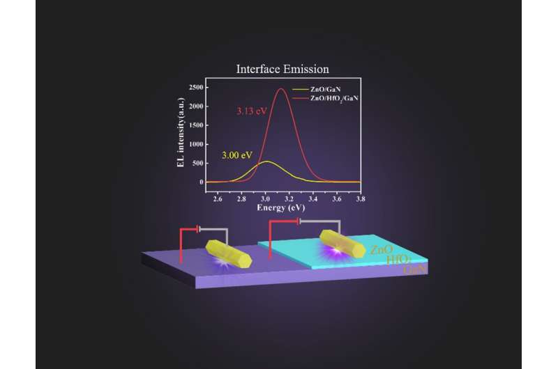
Improvement of the light emitting performance by presenting the nano-buffer layer. Credit: Compuscript Ltd
In a new publication from Opto-Electronic Advances, researchers led by Professor Xu Chunxiang, Southeast University, Nanjing, China discuss nano-buffer controlled electron tunneling to regulate heterojunctional interface emission.
Light emitting diodes (LEDs) are widely used in the field of lighting and display. Homojunction is the best choice when considering interface loss and carrier concentration matching. However, for some semiconductor materials, where it is difficult to obtain homojunction, energy level matching heterostructure is also a choice to build LEDs. Compared with GaN, ZnO has a band gap of 3.37ev, which is similar to GaN. However, its exciton binding energy is as high as 60 meV, which is much larger than room temperature thermal energy (26mev). Therefore its excitons can exist stably at room temperature, which is expected to realize room temperature exciton type light-emitting devices and low threshold laser devices. In 1997, Professor Tang Zikang obtained the optically pumped stimulated emission of ZnO thin films at room temperature; an article about this work published in Science predicted the potential advantages of ZnO in the field of ultraviolet laser devices with "will UV lasers beat the blues?".
Visible interface emission is inevitable in GaN / ZnO light-emitting diodes. Introducing an electron barrier is a common and effective method. In existing research, the appropriate electron barrier layer can effectively block the interface emission, but if it can be used by adjusting the interface emission, it will effectively improve the luminous efficiency of LED.
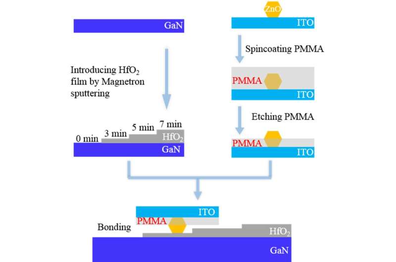
Schematic of device fabrication. Credit: Compuscript Ltd
In view of the problems outlined above, the authors of this paper have systematically studied the regulation of HfO2 electron barrier layer on interface emission in GaN / ZnO structure. They discuss in detail the electric field change, energy band change and electron tunneling characteristics of the device structure after the introduction of ultra-thin HfO2 layer, so as to outline the influence of these on the electroluminescence characteristics of the device. The results show that when the thickness of HfO2 layer is 5.03 nm, the energy band of the device becomes steeper, and a large tunneling current will be generated at the interface between ZnO and HfO2 layer. The interface luminescence wavelength will move from 414 nm to 394 nm, and the overall luminescence intensity of the device will increase about twice.
This paper provides a research method for the interface emission control of semiconductor heterostructures, and a preparation method for obtaining efficient pure color heterostructure light-emitting diodes.
More information: Wei Liu et al, Nano-buffer controlled electron tunneling to regulate heterojunctional interface emission, Opto-Electronic Advances (2021). DOI: 10.29026/oea.2021.200064
Journal information: Science
Provided by Compuscript Ltd


