Tiny nanoparticles improve charge transport

Three-dimensional topological insulators are materials that can conduct electric current without resistance—but only on their surface. However, this effect is difficult to measure. This is because these materials usually have little surface area in relation to their volume, which means their transport properties are dominated by bulk charge carriers.
Bielefeld University physicists have now succeeded in developing topological insulators based on tiny nanoparticles and have thus been able to demonstrate charge transport on the surface. The study was conducted in cooperation with researchers from the University of Duisburg-Essen and the Leibniz Institute for Solid State and Materials Research Dresden. The scientists have published their results today in the journal Small.
Topological insulators have properties that can only be described by quantum physics. What is special about these quantum materials is that their bulk does not conduct electricity at all or only very poorly, while charge carriers can move without interference in protected transport channels on their surface. The compound bismuth telluride is a material with such protected transport channels.
"Macroscopically large samples of these three-dimensional topological insulators, however, have a very high volume compared to their surface area. As a result, there are a lot more bulk charge carriers, which means their poor charge transport dominates over the charge transport on the surface," says Professor Dr. Gabi Schierning from the Thin Films and Physics of Nanostructures research group at Bielefeld University. "Even though the special transport properties of three-dimensional topological insulators are predicted in theory, it is difficult to examine them in experiments."
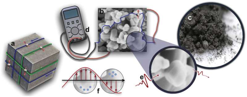
To get around this problem, the scientists are using nanoparticles. Because these particles are so small, they have a large surface area in relation to their volume. Schierning and her colleagues have now compressed nano-particles of bismuth telluride into pellets five millimeters wide and 0.5 millimeters thick—and produced a three-dimensional topological insulator made up of nano units.
Macroscopic material samples with numerous interfaces
"With this trick, we managed to create macroscopic material samples with a high number of interfaces and surfaces. Our study shows that the protected charge carriers on these surfaces can be examined and that electric current is conducted very well there," says Sepideh Izadi, a doctoral student in Schierning's research group and lead author of the study. Schierning adds that their "special material design has made it possible for us to tease out properties that we know from theory but could not see before. That's what makes the work so special for me."
The study was conducted in close cooperation with scientists from the University of Duisburg-Essen and the Leibniz Institute for Solid State and Materials Research Dresden. First, the material samples were prepared in the research group of Professor Dr. Stephan Schulz from the University of Duisburg-Essen. This required a lot of work: the nanoparticles need to have very clean surfaces, for example, and not react with the environment. "They also have to be brought together so that they stick to each other—like building a sandcastle—but at the same time, they must not be compacted so much that the protected transport channels on the interfaces are lost," says Schierning.
The researchers then used various methods to investigate the charge transport on the interfaces and surfaces. Together with colleagues from the Leibniz Institute for Solid State and Materials Research in Dresden, for example, the Bielefeld scientists measured how well the material sample conducts current under different conditions, such as at different temperatures or with different magnetic fields. "The findings are a clear indication of transport mechanisms of a three-dimensional topological insulator," says Schierning.
The investigations were rounded off by terahertz spectroscopy, for which the research team of Professor Dr. Martin Mittendorff from the University of Duisburg-Essen was responsible. In this process, the sample is excited with electromagnetic waves in the terahertz range and the reflected radiation is measured. Here, too, special phenomena were observed that only occur in three-dimensional topological insulators—and even at temperatures as low as about minus 70 degrees Celsius, quite high temperatures for such an effect.
"Our study shows that three-dimensional topological insulators can be realized on a macroscopic scale and show their properties at comparatively high temperatures. This is a significant step in fundamental research, and one which could also be important for potential applications—but we are still a long way from that," says Schierning. Three-dimensional topological insulators could be used in quantum computers, for example.
More information: Sepideh Izadi et al, Interface‐Dominated Topological Transport in Nanograined Bulk Bi 2 Te 3, Small (2021). DOI: 10.1002/smll.202103281
Journal information: Small
Provided by Bielefeld University


