July 5, 2021 feature
Piezoelectric microelectromechanical system-based optical metasurfaces
 Schematic of mirror-like light reflection by the MEMS-OMS before the actuation, i.e., with the initial gap of ~350 nm between the OMS nanobrick arrays and MEMS mirror. Incident light is specularly reflected by the MEMS-OMS regardless the OMS design. (B and C) Schematic of demonstrated functionalities, (B) anomalous reflection and (C) focusing (depending on the OMS design), activated by bringing the MEMS mirror close to the OMS surface, i.e., by decreasing the air gap to ~20 nm. Credit: Science Advances, 10.1126/sciadv.abg5639")
Optical metasurfaces can unprecedently regulate versatile wavefronts at the subwavelength scale. Most well-established optical metasurfaces are, however, static and feature well-defined optical responses that are determined by optical metasurface configurations set during their development. The dynamic configurations of the materials investigated so far often show specific limitations and reduced reconfigurability. In a new report now published on Science Advances, Chao Meng and a research team in nanotechnology, nano-optics, and electronics in Denmark, Norway and China, combined a thin-film piezoelectric micromechanical system (MEMS) with a gap-surface plasmon-based optical metasurface (OMS). Using the setup, they developed an electrically driven, dynamic microelectromechanical system-optical metasurface platform to regulate phases alongside amplitude modulations of the reflected light by finely actuating the MEMS mirror. Using this platform, they showed how the components afforded polarization-independent beam steering and two-dimensional focusing with high modulation efficiencies and fast responses. The platform offers flexible solutions to realize complex dynamics of 2D wavefront regulations with applications in reconfigurable and adaptive optical networks and systems.
Optical metasurfaces
Optical metasurfaces typically represent sub-wavelength dense planar arrays of nanostructured elements also known as meta-atoms that are designed to offer scattered optical fields and local phase regulation. Numerous applications in the past have demonstrated free-space wavefront shaping, versatile polarization transformations, optical vortex generation and optical holography. For more intelligent and adaptive systems including light detection and ranging (LIDAR) as well as free-space optical tracking and communications, or dynamic display and holography, it is highly desirable to develop optical metasurfaces with reconfigurable functionalities. In this work, Chao Meng and a team of scientists combined a thin-film piezoelectric MEMS (micromechanical system) with the gap-surface plasmon-based optical metasurface (OMS) to develop an electrically-driven dynamic MEMS-OMS platform. In the main idea, they facilitated the conventional gap surface plasmon-based optical metasurface to form a moveable back reflector. The scientists designed and developed the OMS and MEMS mirrors to discern the processing paths and then combined them to ensure design freedom on both sides with reduced complexity during development. The work offered a continuously tunable and reconfigurable MEMS-OMS platform with ultracompact dimensions and low power consumption.
 Schematic of the OMS unit cell including the air gap and gold mirror. (B) The complex reflection coefficient r calculated as a function of the nanobrick side length Lx and air gap ta with other parameters being as follows: λ = 800 nm, tm = 50 nm, Λ = 250 nm, and Ly = Lx. Coloration is related to the reflection amplitude, while the magenta lines represent constant reflection phase contours. (C) Reflection phase (dashed lines) and amplitude (solid lines) dependencies on the nanobrick length Lx for two extreme air gaps: ta = 20 nm (red) and 350 nm (blue). Circles represent the nanobrick sizes selected for the OMS supercell designed for dynamic beam steering. (D) Top view and (E) cross section of the designed MEMS-OMS supercell. (F and G) Distributions of the reflected TM electric field (x component) at 800-nm wavelength for air gaps of ta = 20 and 350 nm, respectively. (H) Diffraction efficiencies of different orders (|m| ≤ 1) calculated as a function of the air gap ta for TM/TE incident light with 800-nm wavelength. (I) Diffraction efficiencies of different orders (|m| ≤ 1) calculated at the air gap ta = 20 nm as a function of the wavelength for TM/TE incident light. Credit: Science Advances, 10.1126/sciadv.abg5639")
The experiments
Using this platform, Meng et al. experimentally showed dynamic polarization-independent beam steering and reflective 2D focusing. They electrically actuated the MEMS mirror to regulate the MEMS-CMS distance, and showed polarization-independent dynamic responses with large modulation efficiencies. The device functioned at a wavelength of 800 nm with a beam steering efficiency reaching 40 to 46 percent for transverse magnetic (TM) and transverse electric (TE) polarizations. The proposed device maintained a metal-insulator-metal structure composed of a thick gold layer placed on top of a silicon substrate to form the microelectromechanical systems mirror, while 2D arrays of gold nanobricks on a glass substrate formed the optical metasurface (OMS) structure. The scientists facilitated the proposed functional wavelength in the device and observed the transformation of the reflection phase response to indicate a simple and straightforward approach to realize a MEMS-OMS chip.
Designing the experimental conditions
-
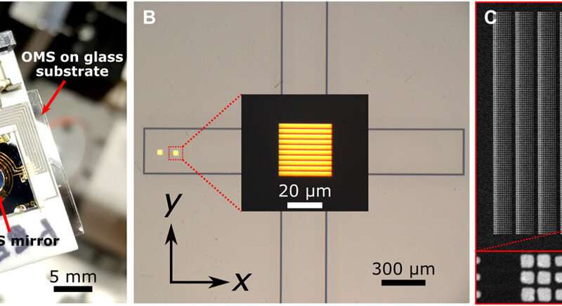
MEMS-OMS assembly. (A) Typical photo of the MEMS-OMS assembly consisting of the OMS patterned on a glass substrate, an ultraflat thin-film MEMS mirror, and a printed circuit board (PCB) for electrical connection. (B) Optical microscopy and (C) SEM images of the OMS representing the 30 μm by 30 μm and 250-nm-period array of differently sized gold nanobricks designed for dynamic beam steering, fabricated atop a 10-μm-high pedestal on the glass substrate, and used in the MEMS-OMS assembly. Photo credit: Chao Meng, University of Southern Denmark. Credit: Science Advances, 10.1126/sciadv.abg5639 -
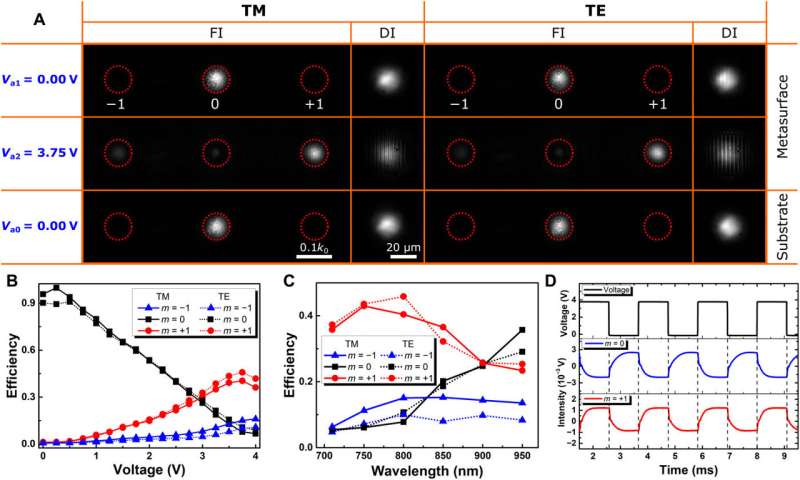
Polarization-independent dynamic beam steering: Characterization. (A) Optical images at the direct object (DI) and Fourier image (FI) planes of the reflected light from MEMS-OMS under actuation voltages of Va1 = 0.00 V (top) and Va2 = 3.75 V (middle) for TM/TE normally incident light with 800-nm wavelength. Reflected light from unstructured substrate (bottom) in the MEMS-OMS device is also recorded as a reference. (B) Diffraction efficiencies of different orders (|m| ≤ 1) measured as a function of the actuation voltage for TM/TE incident light with 800-nm wavelength. (C) Diffraction efficiencies of different orders (|m| ≤ 1) measured as a function of the wavelength for TM/TE incident light. (D) Response time of the different diffraction orders (m = 0/+1) measured by actuating the MEMS mirror with a periodic rectangle signal. Credit: Science Advances, 10.1126/sciadv.abg5639 -
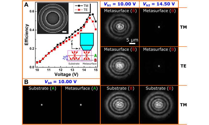
Polarization-independent dynamic 2D focusing: Characterization. (A) Focusing efficiencies measured as a function of the actuation voltage for TM/TE incident light with 800-nm wavelength. The upper-left inset is a typical SEM image of the OMS representing 14-μm-diameter and 250-nm-period array of differently sized gold nanobricks designed for dynamic 2D focusing. Scale bar, 2 μm. The bottom-right inset illustrate the measurement method in which the incident beam is focused at plane A (focal plane of the objective) and impinging on the unstructured substrate or OMS area of the MEMS-OMS at plane B (2f distance away from the focal plane of the objective), resulting in respective divergent or focused reflected fields. (B) Optical images of the reflected light from the unstructured substrate and OMS area of the MEMS-OMS positioned at plane B with actuation voltages of Vb1 = 10.00 V and Vb2 = 14.50 V for TM/TE incident light at 800-nm wavelength. The reflected light from the unstructured substrate and OMS area of the MEMS-OMS positioned at plane A was also recorded as a reference. Credit: Science Advances, 10.1126/sciadv.abg5639
The team then designed a MEMS-OMS platform to realize polarization-independent dynamic beam steering using a separately designed optical micro-lens and an ultrafast MEMS mirror on a printed circuit board. The method simplified the process of development, and they characterized the individual components of the experimental setup using an optical microscope and scanning electron microscope. Following the design and fabrication of the setup, Meng et al. estimated the smallest achievable gap between the MEMS mirror and the OMS substrate surface using multiwavelength interferometry. The value was as small as 100 nm, and the scientists characterized the performance of the MEMS-OMS platform using a wavelength-tunable laser and optical, polarization and imaging components. The thin-film mirror survived more than 1011 cycles for standard operational conditions to accomplish optical, capacitive and piezoresistive sensing, the MEMS device could also maintain a resonance frequency without instability. To understand the dynamic focusing mechanisms behind the MEMS-OMS device, Meng et al. electrically actuated the mirror and observed the corresponding optical responses in the direct object plane and verified the focussing effect using a focussed incident beam.
Outlook
In this way, Chao Meng and colleagues developed an electrically driven dynamic MEMS-OMS platform that combined a thin-film piezoelectric MEMS mirror with optical metasurfaces. The platform offered regulated phase and amplitude modulation of the reflected light by fine actuating the MEMS mirror. The scientists designed and showed the MEMS-OMS devices that function in the near-infrared wavelength range to note fast and efficient function. The experimental setup can be improved by circumventing the requirement to reduce the gap between the MEMS mirror and the OMS surface. Using the device developed in this work, Meng et al. realized diverse functionality and dynamic reconfigurable performance to open fascinating perspectives and realize high-performance, dynamically controlled devices with potential future applications in reconfigurable and adaptive optical systems.
More information: Meng C. et al. Dynamic piezoelectric MEMS-based optical metasurfaces, Science Advances, 10.1126/sciadv.abg5639
Yu N. et al. Flat optics with designer metasurfaces, Nature Materials, doi.org/10.1038/nmat3839
Khorasaninejad et al. Metalenses at visible wavelengths: Diffraction-limited focusing and subwavelength resolution imaging, Science, 10.1126/science.aaf6644
Journal information: Science Advances , Nature Materials , Science
© 2021 Science X Network


