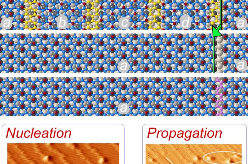
Top panel: Transformation of epitaxial-silicene on ZrB2 from domain structure to single-domain. The labels a,b,c and d represent four different shifts of the silicene lattice resulting from the presence of the dislocations. Silicon atoms in the domains, boundaries and on top of Zr are blue, yellow and red respectively. The Topmost Zr atoms are colored grey. The dark grey Zr atoms are used to visualize the shifts of the domains visualized by the positions of red atoms. They correspond to the positions of red Si atoms for a single-domain a. The green lines compare the positions of the Si atoms before and after merging of four successive domains into a single-domain a through the reaction of 4 dislocations. A row of Si atoms (colored in pink) can then be incorporated into the resulting gap. Bottom panel: STM images showing the path found by nature to resolve this atomistic puzzle. Credit: Japan Advanced Institute of Science and Technology
We might imagine crystals to be perfect structures, but they are, in fact, often plagued with "defects." Curiously enough, such defects often appear due to atoms undergoing reorganization to lower the energy of the system and attain stability.
"Dislocations can strongly affect the physical and chemical properties of a crystal. Moreover, they can undergo "reactions" when for instance strain is applied on the crystal or atoms are added to its surface. Studying how dislocations react can, therefore, provide crucial insights on how to cure these crystal defects. Silicene on zirconium diboride (ZrB2) provides a perfect test bed for that.
This two-dimensional form of silicon features an array of dislocations which disappear when few Si atoms are deposited on top of it. This transformation, that suppresses the high cost of energy caused by the presence of unbounded Si atoms on the surface, requires the reaction of four dislocations to create the room necessary to accommodate the deposited atoms in the silicene sheet. As this needs the motion of a large number of atoms and to overcome the repulsive interaction between the dislocations, this transformation looked very unlikely at first glance: It is a veritable atomistic puzzle which has to be solved to integrate the deposited atoms," says Senior Lecturer Antoine Fleurence from Japan Advanced Institute of Science and Technology (JAIST), Japan, who works on 2D materials.
STM images showing the path found by nature to resolve this atomistic puzzle. Credit: Japan Advanced Institute of Science and Technology
In a new study published in 2D Materials, Dr. Fleurence and his colleague, Prof. Yukiko Yamada-Takamura from JAIST, monitored using scanning tunneling microscopy (STM) the evolution of dislocations in a silicene sheet in real time after depositing silicon (Si) atoms on it.
Through this real time monitoring the trick used by the nature to integrate the deposited Si atoms and obtain a dislocation-free silicene sheet could be determined: the silicene sheet experiences a sequence of dislocation reactions during which the integration of Si atoms within the silicene sheet occurs. Locally "nucleated" single-domain islands then propagate across the entire silicene sheet to eventually result in a dislocation-free, single-domain structure.
"The information on dislocation dynamics provided by this study could be used to find solutions to heal structural defects in similar 2D materials, interfaces, and a wide range of nanomaterials," says Dr. Fleurence.
More information: Antoine Fleurence et al, Adatom-induced dislocation annihilation in epitaxial silicene, 2D Materials (2021). DOI: 10.1088/2053-1583/ac15da
Provided by Japan Advanced Institute of Science and Technology


