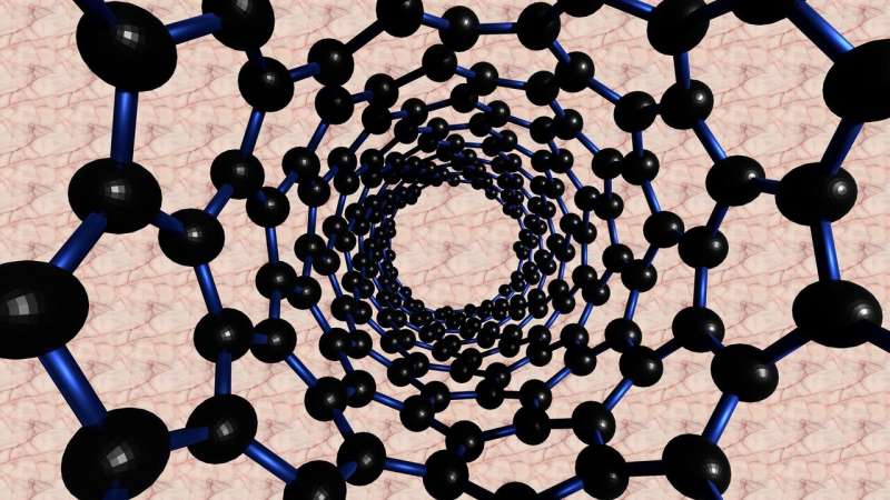
New atomically precise graphene nanoribbon heterojunction sensor developed

An international research team led by the University of Cologne has succeeded for the first time in connecting several atomically precise nanoribbons made of graphene, a modification of carbon, to form complex structures. The scientists have synthesized and spectroscopically characterized nanoribbon heterojunctions. They then were able to integrate the heterojunctions into an electronic component. In this way, they have created a novel sensor that is highly sensitive to atoms and molecules. The results of their research have been published under the title "Tunneling current modulation in atomically precise graphene nanoribbon heterojunctions' in Nature Communications. The work was carried out in close cooperation between the Institute for Experimental Physics with the Department of Chemistry at the University of Cologne, as well as with research groups from Montreal, Novosibirsk, Hiroshima, and Berkeley. It was funded by the German Research Foundation (DFG) and the European Research Council (ERC).
The heterojunctions of graphene nanoribbons are just one nanometer—one millionth of a millimeter—wide. Graphene consists of only a single layer of carbon atoms and is considered the thinnest material in the world. In 2010, researchers in Manchester succeeded in making single-atom layers of graphene for the first time, for which they won the Nobel Prize. "The graphene nanoribbon heterojunctions used to make the sensor are each seven and fourteen carbon atoms wide and about 50 nanometres long. What makes them special is that their edges are free of defects. This is why they are called "atomically precise" nanoribbons," explained Dr. Boris Senkovskiy from the Institute for Experimental Physics. The researchers connected several of these nanoribbon heterojunctions at their short ends, thus creating more complex heterostructures that act as tunneling barriers.
The heterostructures were investigated using angle-resolved photoemission, optical spectroscopy, and scanning tunneling microscopy. In the next step, the generated heterostructures were integrated into an electronic device. The electric current flowing through the nanoribbon heterostructure is governed by the quantum mechanical tunneling effect. This means that under certain conditions, electrons can overcome existing energy barriers in atoms by 'tunneling,' so that a current then flows even though the barrier is greater than the available energy of the electron.
The researchers built a novel sensor for the adsorption of atoms and molecules from the nanoribbon heterostructure. The tunnel current through the heterostructure is particularly sensitive to adsorbates that accumulate on surfaces. That is, the current strength changes when atoms or molecules, such as those of gases, accumulate on the surface of the sensor. "The prototype sensor we built has excellent properties. Among other things, it is particularly sensitive and can be used to measure even the smallest amounts of adsorbates," said Professor Dr. Alexander Grüneis, head of a research group at the Institute of Experimental Physics.
More information: Boris V. Senkovskiy et al, Tunneling current modulation in atomically precise graphene nanoribbon heterojunctions, Nature Communications (2021). DOI: 10.1038/s41467-021-22774-0
Journal information: Nature Communications
Provided by University of Cologne


