April 6, 2021 feature
High-order superlattices by rolling up van der Waals heterostructures

Two-dimensional (2D) materials and van der Waals (vdW) heterostructures are flexible materials with distinct atomic layers beyond traditional units of lattice-matching requirements. Nevertheless, the 2D van der Waals structures researchers have hitherto explored are limited to relatively simple heterostructures with a small number of blocks. It is exponentially more difficult to prepare high-order vdW superlattices with a myriad of alternating units due to their limited yield and the material damage associated with restacking or synthesis.
Using the capillary-force-driven rolling-up process, Zhao et al. delaminated synthetic tin sulfide (SnS2)/tungsten diselenide (WSe2) van der Waals heterostructures from the growth substrate to produce roll-ups with alternating monolayers of the materials to create high-order SnS2/ WSe2 vdW superlattices. The superlattices modulated the electronic band structure and dimensionality to allow the transition of transport characteristics from semiconducting to metallic, and from 2D to one-dimensional (1D) with an angle-dependent linear magnetoresistance. The team extended this strategy to create diverse 2D/2D vdW superlattices that are more complex and beyond mere 2D, including 3D thin-film materials and 1D nanowires to generate a mixture of mixed-dimensional vdW superlattices. The work indicated a general approach to produce high-order vdW superlattices with a range of materials compositions, dimensions, chirality and topology to develop a rich material platform for fundamental studies and technical applications. The results are now published on Nature.
Creating van der Waals heterostructures.
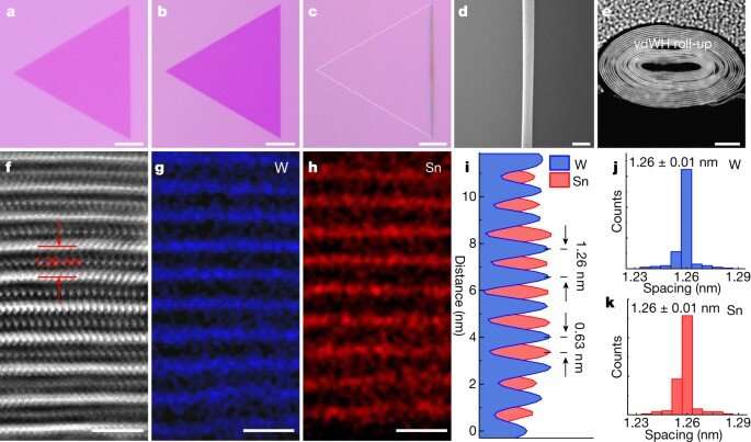
Atomically thin, 2D layered materials have opened new avenues to explore low-dimensional physics at the limit of single or few atomic layers, to create functional devices with unprecedented performance or unique functionalities. Materials scientists can mix and match distinct 2D materials including graphene, hexagonal boron nitride and transition metal dichalcogenides to create 2D vdW heterostructures and vdW superlattices beyond the limits of lattice matching. These materials architectures introduced a paradigm to engineer artificial materials with structural and electronic properties for functions beyond the reach of existing materials. Researchers had thus far obtained vdW heterostructures and superlattices via a series of methods including chemical vapor deposition (CVD), mechanical exfoliation and layer-by-layer restacking to create diverse heterostructures. In this work, Zhao et al. reported a straightforward approach to create high-order vdW superlattices by rolling up 2D vdW heterostructures. The scientists exposed the CVD-grown 2D/2D vdW heterostructures to an ethanol-water-ammonia solution to allow the capillary force to drive spontaneous delamination and rolling-up processes to form vdW heterostructure roll-ups. These materials contained high-order vdW superlattices without multiple transfer and restacking processes. The team then used scanning transmission electron microscopy (STEM) and energy-dispersive X-ray spectroscopy (EDS) elemental mapping studies to determine the atomic composition of the superlattices.
Developing roll-up vdW heterostructures
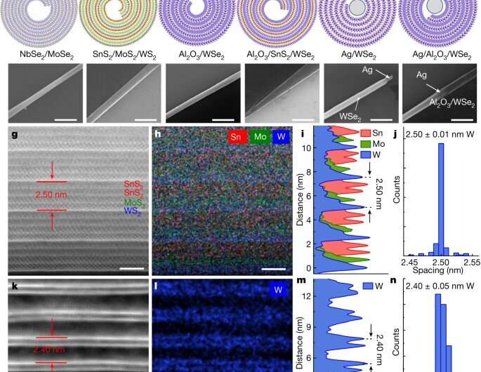
The scientists next conducted electrical transport studies to show the evolution of the transport characteristics from 2D to 1D with greatly enhanced conductance and angle-dependent magneto-resistance in the vdW superlattices. They extended the rolling-up strategy to create diverse 2D/2D vdW superlattices and complex three-component 2D/2D/2D vdW superlattices using tin-sulfide/molybdenum disulfide/tungsten disulfide materials. The technique also allowed the production of materials beyond 2D, including 3D or 1D materials to generate a range of multi-dimensional vdW superlattices.
Fabrication process
During the fabrication process of roll-up vdW superlattices, Zhao et al. first grew a 2D atomic crystal on a silicon dioxide silicon substrate using a modified chemical vapor deposition process. The team used the resulting 2D crystals as templates for vdW epitaxial growth to achieve vdW heterostructures. They then initiated capillary-force-driven rolling-up processes using ethanol-water-ammonia solution. The solution intercalated at the interface between the tin sulfide/tungsten disulfide vdW heterostructures and the underlying silicon dioxide/silicon substrate to delaminate the tin-sulfide/tungsten diselenide constructs and induce spontaneous rolling-up processes with the help of surface tension. The work enabled 2D vdW heterostructure rollups containing high-order 2D vdW superlattices. The researchers then used focused-ion-beam milling to produce a cross-sectional slice of the roll-ups, and analyzed them using high-resolution STEM and EDS elemental mapping studies.

New materials properties
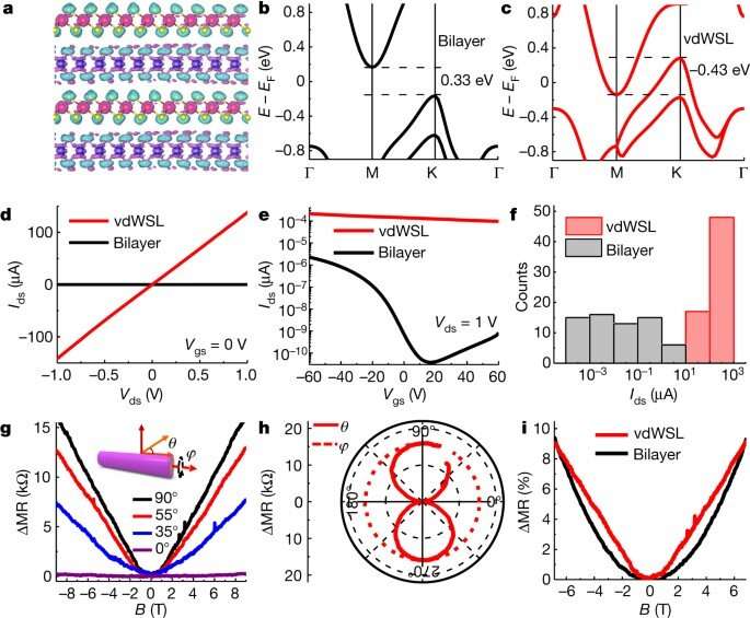
The rolling-up process opens a straightforward path for high-order superlattices and provides materials scientists a method to tailor the interlayer coupling, dimensionality and topology of the resulting superlattice structure. For example, by transforming the tin-sulfide/tungsten diselenide bilayer vdW heterostructures into a high-order vdW superlattice, Zhao et al. could modify its band structure and therefore its electronic properties. The researchers explored the effects by conducting first-principles calculations based on many-body perturbation theory and probed the electronic band structure of the resulting vdW superlattices. The outcomes showed the heterobilayer to exhibit a type-II band alignment with the valence band maximum (VBM) coming from the tungsten selenide material and the conduction band minimum coming from the tin sulfide for an apparent indirect bandgap of 0.33 eV. Additional structural alterations of superlattices could change the profile from mostly superconducting characteristics in heterobilayers to metallic behavior.

Field-effect transistors
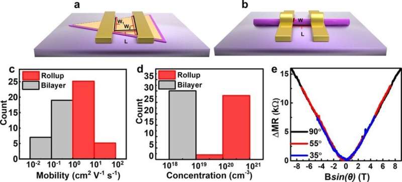
To understand the electrical properties of the vdW superlattices, the researchers next developed field-effect transistors (FETs) using the heterobilayers and roll-up vdW superlattices on silicon dioxide/silicon substrate, with thin metallic films as the source and drain electrodes, a silicon substrate as the back gate and silicon dioxide as the gate dielectric of the setup during electrical transport studies. The heterobilayer device showed little conduction, while the roll-up vdW superlattices showed high conductance with a current of 100 µA at 1 V bias. The results highlighted the greatly improved charge transport in the roll-up vdW superlattices due to the substantially reduced bandgap. Based on the transfer characteristics, Zhao et al. determined the carrier mobility and carrier density in the vdW heterobilayer and roll-up superlattices. The work indicated a band structure evolution. Notably, the team showed how the dimensionality altered from 2D to 1D upon rolling-up. They confirmed the 1D transport nature of the roll-ups using angle-dependent magnetoresistance studies.
High-order superlattices.
Zhao et al. next extended the roll-up strategy to produce 2D/2D superlattice roll-ups with distinct chemical compositions and physical properties as a rich platform to investigate ferroelectricity, ferromagnetism, superconductivity and piezoelectricity under diverse geometries and dimensionalities. They also developed high-order superlattice structures containing repeating units of monolayers and bilayers to form a highly uniform superlattice structure for the three constituent 2D materials. They extended the approach to create mixed-dimensional vdW superlattices based on atomic layer deposition (ALD). The researchers also developed more complex superlattices by rolling up the heterobilayer with different material compositions and chiralities to present an exciting direction to explore in future studies.

Outlook
In this way, Bei Zhao and colleagues developed a straightforward and general approach to form multi-dimensional high-order vdW superlattices containing alternating layers of distinct 2D materials, alongside 3D and 1D materials. The materials maintained widely variable compositions and dimensions to create highly engineered artificial constructs beyond traditional materials systems. The work provides considerable freedom to tailor the resulting superlattice structures for interlayer coupling, chirality and topology. Such materials can be tuned to produce complex superlattice structures resembling those typically used in multi-sheet transistors, quantum tunneling devices, advanced light-emitting diodes, or quantum cascading lasers. This experimental setup with 1D and 3D components offer unique geometries that are useful to explore quantum physics and realize specific device functions. The work also provides a rich material platform for fundamental studies and technical applications.
More information: Zhao B. et al. High-order superlattices by rolling up van der Waals heterostructures, Nature, doi.org/10.1038/s41586-021-03338-0.
Novoselov K. S. et al. 2D materials and van der Waals heterostructures, Science, 10.1126/science.aac9439
Saito Y. et al. Highly crystalline 2D superconductors, Nature Reviews Materials, doi.org/10.1038/natrevmats.2016.94
Provided by Science X Network
© 2021 Science X Network


