January 11, 2021 feature
Self‐folding 3-D photosensitive graphene architectures

Stimuli-responsive, self-folding, two-dimensional (2-D) layered materials have interesting functions for flexible electronics, wearables, biosensors, and photonics applications. However, limits with scalability and a lack of design tools can prevent high integration and their reliable function. In a new report now published on Advanced Intelligent Systems, Qi Huang, and a team of scientists in chemical and biomolecular engineering and electrical and computer engineering at Johns Hopkins University, U.S., proposed a mass-production strategy to create monolayer graphene-based reversible self-folding structures. The material can be used in microfluidics and micromechanical systems. As proof of concept, they achieved complex and functional devices in the form of rings, polyhedra, flowers and origami birds. They then integrated gold electrodes to the constructs to improve their detection sensitivity. The experiments suggest a comprehensive framework to rationally design and fabricate scalable and complex, 3-D, self-folding optical and electronic devices by folding 2-D monolayer graphene.
Developing 3-D microstructures from 2-D precursors
The development of 3-D integrated microstructures from wafer-scale, 2-D precursors can be useful across a variety of fields including optics, electronics, robotics and biomedical engineering. However, it is yet difficult to realize wafer-scale on-chip or free-standing and reversible 2-D layered material-based hybrid devices. In this work, Huang et al. investigated the folding mechanics of differentially cross-linked SU8—i.e., an epoxy-based ultraviolet (UV) cross-linkable, negative photoresist based on a commercial resin, and the interaction of light with flexible graphene-gold (Au)-SU8 3-D microstructures. The team used experiments and simulations to introduce several new ideas and demonstrated the self-folding SU8 graphene microstructures. They varied the extent of SU8 crosslinking by tuning the UV dose to develop a physics-based, coarse-grained model that encompassed the effect of UV light for material mechanics and volume changes. They then used the approach to provide example 3-D shapes including origami birds. The method also included multilayer very-large-scale integration (VLSI) computational approaches. The method allowed simple connections with electrodes and other electronic, optical or microfluidic modules. The studies displayed 3-D graphene hybrid functional devices suitable for robotics, wearables and photonics.

Rationally designing 3-D self‐folding SU8 structures
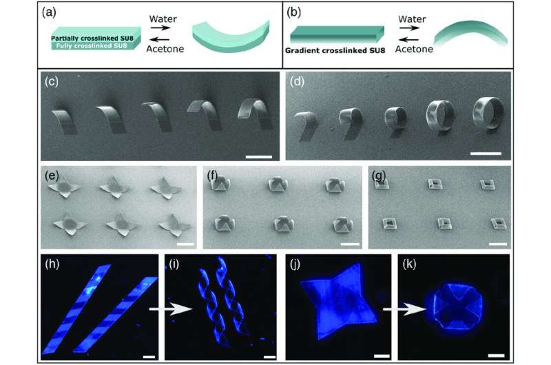
Huang et al. tested two methods to allow reversible folding of differentially cross-linked SU8 films including bilayer and gradient methods. For both versions, they first deposited a 50 nm thick thermally evaporated copper sacrificial layer on a wafer or glass slide. During the bilayer method, they patterned SU8 bilayer films with a fully cross-linked bottom layer and a partially crosslinked top layer using photolithography to facilitate bending away from the wafer. They then spin-coated the SU8 layers on to the material and conditioned the bilayer patterns by immersing them in acetone to create self-folding precursors. The conditioned structures could reversibly fold and unfold on solvent transfer from acetone to water. By varying the thickness of the pattern, they assembled curved beams with different radii and a variety of 3-D shapes. The team also varied the dose of UV exposure ratio to increase the extent of pattern folding. They noted how different fold angles could be achieved by varying the thickness and extent of cross-linking. The work provided the design criteria required to achieve controlled bending and geometries for SU8 microstructures. The simulations were accurate reproductions of the experimental folding shapes.
Converting graphene into 3-D shapes based on the self-folding SU8 structures
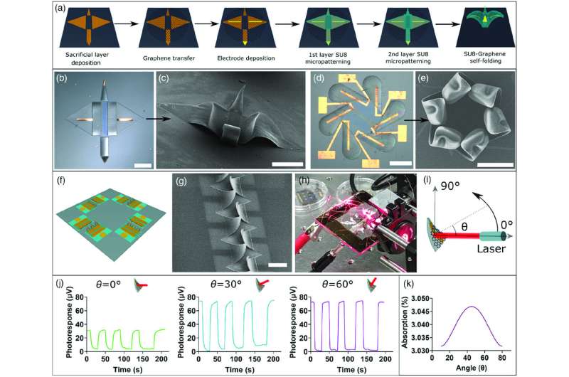
The self-folding structures could importantly support the transformation of flat monolayer graphene into 3-D shapes. This integration process included a few key steps. At first, the team transferred the monolayer graphene grown using chemical vapor deposition from a copper-coated wafer to the sacrificial copper-coated silicon substrate by using the polymethyl methacrylate (PMMA) method. Then using Raman spectra, Huang et al. noted the peaks corresponding to monolayer graphene deposited on SU8 as expected. Thereafter, they patterned graphene via photolithography and plasma etching, and realized self-rolling of graphene-SU8 structures with reversible rolling/unrolling in water and acetone. This integration process of self-rolling graphene-SU8 occurred on a wafer scale, facilitating the inclusion of other elements including gold lines or patterns, to form functional electronic or optical devices.

Developing ultrathin shape-changing smart materials.
Materials scientists typically study graphene for its electronic and optical applications based on unique physical characteristics, high mechanical strength, and stability of the material. Due to its characteristic properties of optoelectronics, the high charge carrier mobility of graphene at ambient temperatures revealed potential applications in high-frequency and high-speed devices. Nevertheless, light absorption and light-matter interaction of graphene is low for atomically thin planar graphene-based devices. Huang et al. therefore leveraged the optical transparency of SU8 to develop 3-D self-folding graphene-based optical devices to form flexible optical devices and wearables. They created multi-rolled 3-D graphene structures to overcome the limits of poor absorptivity of single-layer graphene. The scientists then used a flat graphene-gold-SU8 photodetector and tested the substrate by illuminating each gold electrode with a 488 nm laser. The photovoltage was larger when the laser illumination was directly incident on the graphene side compared to the SU8 side. The reduced illumination resulted from absorption of light in the SU8 film. The photovoltage generated in the work mainly resulted from the gold and graphene overlapping area.
Forming chip-integrated 3-D grapahene-SU8 structures and photodetectors
As proof of concept, Huang et al. developed complex origami-inspired designs and chip-integrated structures. To assemble them, they patterned the copper sacrificial layer and graphene and controlled the UV exposure in specific regions to selectively fold the SU8 microstructure, while other parts remained pinned down flat. Such complex structures will be important for soft robotics with a graphene-gold interface for remote optical energy harvesting applications. The on-chip assembled designs are also important in optoelectronics, which Huang et al. illustrated using angle-resolved photodetectors with a self-folded SU8 graphene photodetector array. Using light illumination, they showed different photoresponses based on the angle of the laser and the material's architecture. The team also used simulations to determine the angle-resolved response.

Outlook
In this way, Qi Huang and colleagues developed a highly parallel process to assemble 3-D flexible graphene microstructures. The method has three key advantages to offer,
- Free-standing materials and chip-integration
- Highly parallel integration of flexible and transparent 3-D graphene devices, and
- Reversible reconfiguration.

The optically transparent photoresist can be spin-coated and maintained with relative flexibility. The structures were stable in air and can form better lightweight alternatives to silicon-based modules for integration in flying and swimming robots. The primary basis of the self-folding mechanism relied on chemical-solvent driven differential swelling to faciliate folding/unfolding motions. The team expect to use this approach to create a range of 3-D microstructures for wearables, moving robots, in biosensors and in energy harvesting devices.
More information: Huang Q. et al. Solvent Responsive Self‐Folding of 3D Photosensitive Graphene Architectures, Advanced Intelligent Systems, doi: doi.org/10.1002/aisy.202000195
Freitag M. et al. Photoconductivity of biased graphene, Nature Photonics, doi: doi.org/10.1038/nphoton.2012.314
Koppens F. H. L. et al. Photodetectors based on graphene, other two-dimensional materials and hybrid systems, Nature Nanotechnology, doi.org/10.1038/nnano.2014.215
Journal information: Nature Photonics , Nature Nanotechnology
© 2021 Science X Network


