Engineering discovery challenges heat transfer paradigm that guides electronic and photonic device design

A research breakthrough from the University of Virginia School of Engineering demonstrates a new mechanism to control temperature and extend the lifetime of electronic and photonic devices such as sensors, smart phones and transistors.
The discovery, from UVA's experiments and simulations in thermal engineering research group, challenges a fundamental assumption about heat transfer in semiconductor design. In devices, electrical contacts form at the junction of a metal and a semiconducting material. Traditionally, materials and device engineers have assumed that electron energy moves across this junction through a process called charge injection, said group leader Patrick Hopkins, professor of mechanical and aerospace engineering with courtesy appointments in materials science and engineering and physics.
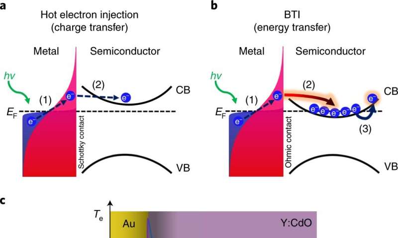
Charge injection posits that with the flow of the electrical charge, electrons physically jump from the metal into the semiconductor, taking their excess heat with them. This changes the electrical composition and properties of the insulating or semiconducting materials. The cooling that goes hand-in-hand with charge injection can significantly degrade device efficiency and performance.
Hopkins' group discovered a new heat transfer path that embraces the benefits of cooling associated with charge injection without any of the drawbacks of the electrons physically moving into the semiconductor device. They call this mechanism ballistic thermal injection.
As described by Hopkins' advisee John Tomko, a Ph.D. student of materials science and engineering: "The electron gets to the bridge between its metal and the semiconductor, sees another electron across the bridge and interacts with it, transferring its heat but staying on its own side of the bridge. The semiconducting material absorbs a lot of heat, but the number of electrons remains constant."
"The ability to cool electrical contacts by keeping charge densities constant offers a new direction in electronic cooling without impacting the electrical and optical performance of the device," Hopkins said. "The ability to independently optimize optical, electrical and thermal behavior of materials and devices improves device performance and longevity."
Tomko's expertise in laser metrology—measuring energy transfer at the nanoscale—revealed ballistic thermal injection as a new path for device self-cooling. Tomko's measurement technique, more specifically optical laser spectroscopy, is an entirely new way to measure heat transfer across the metal-semiconductor interface.
"Previous methods of measurement and observation could not decompose the heat transfer mechanism separately from charge injection," Tomko said.
For their experiments, Hopkins' research team selected cadmium oxide, a transparent electricity-conducting oxide that looks like glass. Cadmium oxide was a pragmatic choice because its unique optical properties are well suited to Tomko's laser spectroscopy measurement method.
Cadmium oxide perfectly absorbs mid-infrared photons in the form of plasmons, quasiparticles composed of synchronized electrons that are an incredibly efficient way of coupling light into a material. Tomko used ballistic thermal injection to move the light wavelength at which perfect absorption occurs, essentially tuning the optical properties of cadmium oxide through injected heat.
"Our observations of tuning enable us to say definitively that heat transfer happens without swapping electrons," Tomko said.
Tomko probed the plasmons to extract information on the number of free electrons on each side of the bridge between the metal and the semiconductor. In this way, Tomko captured the measurement of electrons' placement before and after the metal was heated and cooled.
The team's discovery offers promise for infrared sensing technologies as well. Tomko's observations reveal that the optical tuning lasts as long as the cadmium oxide remains hot, keeping in mind that time is relative—a trillionth rather than a quadrillionth of a second.
Ballistic thermal injection can control plasmon absorption and therefore the optical response of non-metal materials. Such control enables highly efficient plasmon absorption at mid-infrared length. One benefit of this development is that night vision devices can be made more responsive to a sudden, intense change in heat that would otherwise leave the device temporarily blind.
"The realization of this ballistic thermal injection process across metal/cadmium oxide interfaces for ultrafast plasmonic applications opens the door for us to use this process for efficient cooling of other device-relevant material interfaces," Hopkins said.
Tomko first-authored a paper documenting these findings. Nature Nanotechnology published the team's paper, Long-lived Modulation of Plasmonic Absorption by Ballistic Thermal Injection, on November 9; the paper was also promoted in the journal editors' News and Views. The Nature Nanotechnology paper adds to a long list of publications for Tomko, who has co-authored more than 30 papers and can now claim first-authorship of two Nature Nanotechnology papers as a graduate student.
The research paper culminates a two-year, collaborative effort funded by a U.S. Army Research Office Multi-University Research Initiative. Jon-Paul Maria, professor of materials science and engineering at Penn State University, is the principal investigator for the MURI grant, which includes the University of Southern California as well as UVA. This MURI team also collaborated with Josh Caldwell, associate professor of mechanical engineering and electrical engineering at Vanderbilt University.
The team's breakthrough relied on Penn State's expertise in making the cadmium oxide samples, Vanderbilt's expertise in optical modeling, the University of Southern California's computational modeling, and UVA's expertise in energy transport, charge flow, and photonic interactions with plasmons at heterogeneous interfaces, including the development of a novel ultrafast-pump-probe laser experiment to monitor this novel ballistic thermal injection process.
More information: John A. Tomko et al, Long-lived modulation of plasmonic absorption by ballistic thermal injection, Nature Nanotechnology (2020). DOI: 10.1038/s41565-020-00794-z
Journal information: Nature Nanotechnology
Provided by University of Virginia School of Engineering and Applied Science


