Universal three-dimensional crosslinker for all-photopatterned electronics

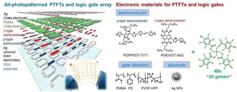
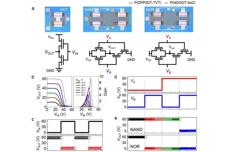
A research team, affiliated with South Korea's Ulsan National Institute of Science and Technology (UNIST) has succeeded in fabricating highly integrated arrays of PTFTs and logic gates via all-solution processing.
A technology to lower the production cost of electronic devices, such as large-area OLEDs that make large TVs has been developed. Instead of expensive vacuum equipment, this technique uses a series of solution processes for the production of electronic devices.
A research team, jointly led by Professor BongSoo Kim in the School of Natural Science, Professor Jeong Ho Cho from Yonsei University, Professor Moon Sung Kang from Sogang University has succeeded in fabricating highly integrated arrays of polymer thin-film transistors and logic gates entirely via all-solution processing technique. The key to this technique is that it uses a highly efficient crosslinking agent that does not yield degradation in the electrical properties of the host materials.
Solution processing technique refers to a fabrication method whereby the materials are dissolved in a variety of solvents, and then they can be coated by spin coating for lab-sized experiments or inkjet printing. Such technique is less expensive than vacuum equipment, yet the disadvantage is that there is the possibility for material damage. In general, the manufacturing process of electronic devices requires stacking of various electronic component layers. And this may increase the risk of material damage, especially when stacking the layers on top of each other by series of solution processing steps. Besides, the heat produced from removing solvents may induce the denaturation of the host materials, which is a major obstacle in realizing all-solution-processed electronic devices.

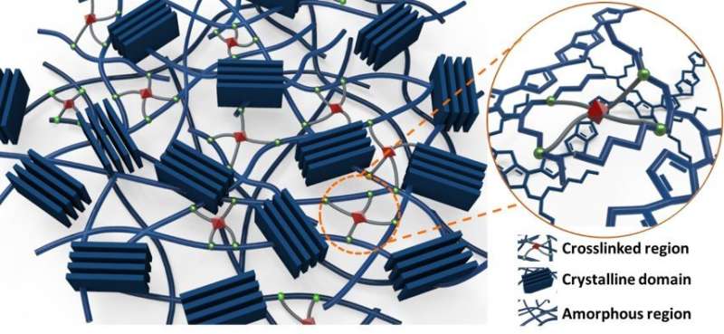
The research team solved such issues, using a three-dimensional crosslinker in tetrahedral geometry containing four photocrosslinkable azide moieties, referred to as 4Bx. This crosslinking agent links the different types of electronic materials (i.e., polymer semiconductors, polymer insulators, and metal nanoparticles), and thus holding them firmly together, like a bridge. Because the crosslinked electronic component layers are strongly resistant to chemical solvents, micropatterning the layers at high resolution as well as stacking the layers on top of each other by series of solution processing steps is possible.

"Crosslinking agents are electrically non-conductive, and therefore the addition of a large amount of a crosslinking agent leads to a morphological change in the film and deterioration in the electrical and optoelectronic properties of the material," says Professor Kim. "However, the new crosslinker can be applied to the patterning process of various solution-processable materials with use of a very low amount is thus highly desirable. Using a very small amount of 4Bx, the research team has succeeded in fabricating highly integrated arrays of polymer thin-film transistors (PTFTs) and logic circuits via all-solution processing. The results show that the PTFTs based on photocrosslinked polymer films show equivalent performance and better stability compared with those prepared using polymer films without the crosslinker. "Overall, this work demonstrates an effective route to all-solution-processed organic electronic devices based on a single fabrication protocol," says Professor Kim.
The findings of this research have been published in the online version of Nature Communications.
More information: Min Je Kim et al. Universal three-dimensional crosslinker for all-photopatterned electronics, Nature Communications (2020). DOI: 10.1038/s41467-020-15181-4
Journal information: Nature Communications


