Credit: American Chemical Society
Multimaterial fibers that integrate metal, glass and semiconductors could be useful for applications such as biomedicine, smart textiles and robotics. But because the fibers are composed of the same materials along their lengths, it is difficult to position functional elements, such as electrodes or sensors, at specific locations. Now, researchers reporting in ACS Central Science have developed a method to pattern hundreds-of-meters-long multimaterial fibers with embedded functional elements.
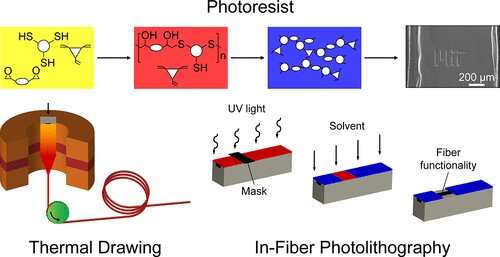
Youngbin Lee, Polina Anikeeva and colleagues developed a thiol-epoxy/thiol-ene polymer that could be combined with other materials, heated and drawn from a macroscale model into fibers that were coated with the polymer.
When exposed to ultraviolet light, the polymer, which is photosensitive, crosslinked into a network that was insoluble to common solvents, such as acetone.
By placing "masks" at specific locations along the fiber in a process known as photolithography, the researchers could protect the underlying areas from UV light. Then, they removed the masks and treated the fiber with acetone.
The polymer in the areas that had been covered dissolved to expose the underlying materials. As a proof of concept, the researchers made patterns along fibers that exposed an electrically conducting filament underneath the thiol-epoxy/thiol-ene coating.
The remaining polymer acted as an insulator along the length of the fiber.
In this way, electrodes or other microdevices could be placed in customizable patterns along multimaterial fibers, the researchers say.
More information: Selectively Micro-Patternable Fibers via In-Fiber Photolithography, ACS Central Science (2020). pubs.acs.org/doi/abs/10.1021/acscentsci.0c01188
Journal information: ACS Central Science
Provided by American Chemical Society


