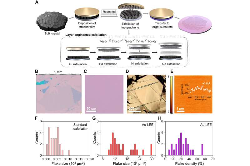
Layer-engineered exfoliation LEE of millimeter-size monolayer graphene. (A) Schematic illustration of our layer-engineered large-area graphene exfoliation technique. The inset shows the change in the number of layers of exfoliated graphene according to the relative binding energy between graphite and a metal stressor film. (B and C) Low- and high-magnification OM images of millimeter-size monolayer graphene obtained by the LEE method. (D and E) OM and AFM images of the cleaved natural graphite surface. The inset is a single trace of the AFM image showing the roughness of LEE-graphene, where the root mean square value is approximately 3.5 Å. (F to H) Histograms of the size and density of monolayer graphene obtained by the standard exfoliation and LEE methods for 25 samples each. Credit: Science Advances, doi: 10.1126/sciadv.abc6601
Large-scale manufacturing processes that aim to produce two-dimensional materials (2DMs) for industrial applications are based on a competition between quality and productivity. The top-down mechanical cleavage method allows pure and perfect 2DMs, but they are a weak option for large-scale manufacture. In a new report in Science Advances, Ji-Yun Moon and a research team in energy systems, materials science, physics and nanoarchitectonics in the U.K., Japan and Korea presented a layer-engineered exfoliation technique to obtain large-scale graphene of up to a millimeter with selective thickness control. Using detailed spectroscopy and electron transport measurement analysis, the team supported the proposed spalling (fragmenting) mechanism. The layer-engineered exfoliation method will pave the way to develop an industrial process for graphene and other 2DMs, for applications in electronics and optoelectronics.
New methods to obtain monolayer graphene
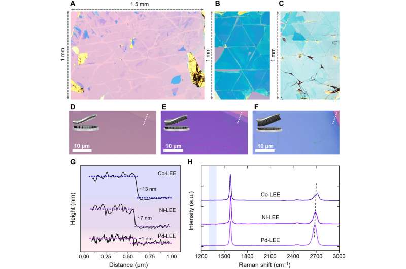
Materials scientists first successfully separated monolayer graphene from three-dimensional (3-D) graphite using top-down mechanical exfoliation. Graphene is a unique material due to its physical and chemical composition that have attracted great attention for diverse applications in electronics, optoelectronics and other fields. In this work, Moon et al. introduced a new technique known as layer-engineered exfoliation (LEE) to obtain large-area graphene while controlling the selective number of graphene layers in the setup. To accomplish this, they deposited a thin film of gold (Au) on pre-cleaved graphite to selectively peel off the topmost monolayer of graphene. They then adjusted the interfacial toughness of graphene by depositing different metal films including palladium (Pd), nickel (Ni) and cobalt (Co) to obtain large-area graphene with a controlled number of layers. Mechanically exfoliated graphene is limited by its size, yield and thickness control, which is not suited for industrial applications at present. Researchers had previously considered vapor deposition, but the results were not outstanding. If a new technique can overcome conventional methods of exfoliation, researchers will have an attractive, alternative synthetic approach to prepare graphene.
Spalling depth control by adjusting the interfacial toughness. (A to C) Low-magnification and (D to F) high-magnification OM images of layer-engineered millimeter-size graphene prepared using Pd, Ni, and Co, respectively, on 300-nm SiO2/Si substrates. (G) AFM line profiles corresponding to the white dashed lines in (D) to (F). (H) Raman spectra of layer-engineered multilayer graphene obtained using Pd, Ni, and Co. a.u., arbitrary units. Credit: Science Advances, doi: 10.1126/sciadv.abc6601
The experiment—LEE of graphene
The scientists used spectroscopy and electron transport studies to confirm the absence of any intrinsic defects or chemical contamination in the samples developed by the LEE method. The exfoliation method is a promising approach to build large-area 2-D heterostructures for commercialization. During the process of graphite flake exfoliation, the team bent the surface using an external stressor to create a crack at domain boundaries, which propagated along the metal-graphene interface to cause large-area exfoliation due to residual tension. For instance, when the team used a gold (Au) film as a stressor, the bending energy between Au-graphene and graphene-graphene allowed the separation of a monolayer without physical defects. Moon et al. quantitatively analyzed the size and density of exfoliated monolayer graphene to verify the reliability of the technique. The outcomes showed an average area that reached a 4,200-fold increase compared to graphene exfoliated via conventional methods. The LEE method also showed better results compared to standard mechanical exfoliation relative to the density of the monolayer. The method was reproducible and therefore reliable to exfoliate monolayer graphene in a controlled approach in the lab.
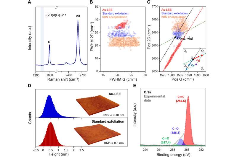
Characterization of monolayer graphene obtained by LEE. (A) Raman spectra of LEE-graphene under 532-nm excitation. (B and C) Γ2D versus ΓG and ω2D versus ωG recorded on three different samples: prepared by Au-LEE (red circles), standard exfoliation (blue circles), and hBN encapsulation (orange circles). (D) Surface roughness of monolayer graphene obtained by LEE and standard exfoliation scanned over 9 μm2. The insets show the corresponding 3D AFM images. Brown-to-yellow scale, 0 to 5 nm. (E) X-ray photoemission spectroscopy (XPS) patterns (C 1s) obtained from LEE-graphene. RMS, root mean square roughness. Credit: Science Advances, doi: 10.1126/sciadv.abc6601
Characterizing LEE graphene
Moon et al. conducted Raman spectroscopy measurements on LEE-graphene to support their proposed mechanism of fragmentation, which was sensitive to stress-induced spalling (fragmentation) of graphene. The results specified how the tensile strain was released during the LEE process when graphene was lifted to recover the pristine property of normally exfoliated graphene. Using additional spectroscopy and microscopy studies, the team confirmed the quality of LEE-graphene. For example, atomic force microscopy (AFM) measurements showed no notable physical defects on the graphene surface, such as cracks, folds or tearing. As a result, they acknowledged that the metal film effectively protected the surface of graphene from organic residues during the LEE process.
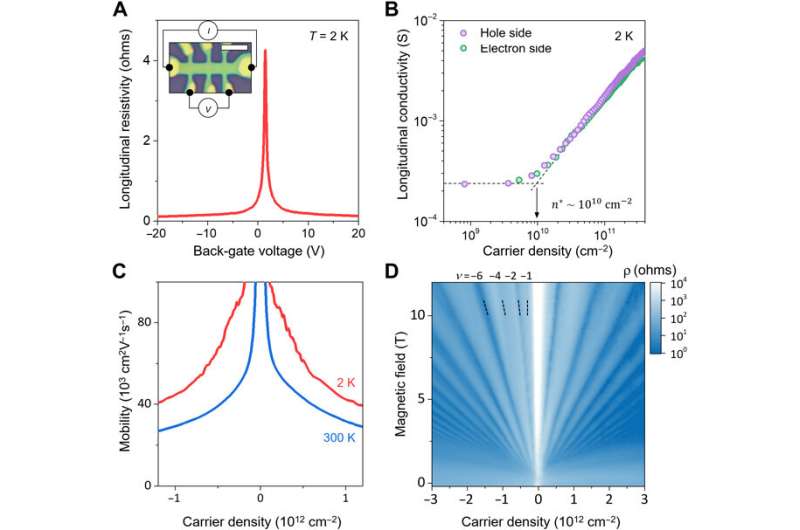
Transport characteristics of hBN-encapsulated LEE-graphene. (A) Longitudinal resistivity as a function of back-gate voltage at 2 K (the CNP is at 1.5 V). The left inset shows an optical micrograph of the device with a wiring schematic for current and voltage measurements. Scale bar, 5 μm. (B) Density dependence of the longitudinal conductivity on a log scale at 2 K. The value of n* extracted from our graphene device is ~1010 cm−2. (C) Electron mobility as a function of carrier density at 2 K (red line) and 300 K (blue line). The mobility is approximately 20,000 cm2V−1 s−1 at 300 K. (D) Map of the longitudinal resistivity as a function of the applied magnetic field and carrier density at 2 K. The well-developed Landau levels indicate that the graphene device is of high quality (black dashed lines indicate filling factors of −1, −2, −4, and −6). Credit: Science Advances, doi: 10.1126/sciadv.abc6601
Electron transport properties in LEE-graphene
The scientists cross-checked the quality of LEE-graphene as evidenced with spectroscopy and microscopy results by conducting electron transport measurements on the monolayer graphene device. They accomplished this by encapsulating graphene between defect-free hexagonal boron nitride (hBN) crystals. The hBN provided a flat and clean surface for graphene and protected the material against contamination after exfoliation. The potential fluctuation value of the graphene device was similar to an adequately exfoliated graphene device in previous work, demonstrating the accuracy of the device developed in this work. The team calculated the electron mobility (µ) of the device at 300 K, which surpassed the magnitude reported for a graphene device in previous work, while matching the mobility of a graphene device developed by the standard exfoliation method elsewhere. The work therefore showed that the LEE technique did not degrade the quality of graphene.
In this way, Ji-Yun Moon and colleagues used and reviewed the LEE (layer-engineered exfoliation) approach to obtain high density graphene with an extraordinarily large area from natural graphite. To accomplish this, they used different metal deposition techniques to control the depth of fragmentation and produce layer-engineered graphene on a large scale. The new method deviated from the standard method of exfoliation, which only allowed a single peeling process. The scientists obtained the large-area graphene from the same graphite flake by repeating the deposition-and-tearing process of the metal film. The work showed how layer-engineered graphene can be exfoliated across a large area, paving the way to large-scale manufacturing for future industrial applications of 2-D heterostructures.
More information: Ji-Yun Moon et al. Layer-engineered large-area exfoliation of graphene, Science Advances (2020). DOI: 10.1126/sciadv.abc6601
F. Wang et al. Gate-Variable Optical Transitions in Graphene, Science (2008). DOI: 10.1126/science.1152793
Jian-Hao Chen et al. Intrinsic and extrinsic performance limits of graphene devices on SiO2, Nature Nanotechnology (2008). DOI: 10.1038/nnano.2008.58
Journal information: Science Advances , Science , Nature Nanotechnology
© 2020 Science X Network


