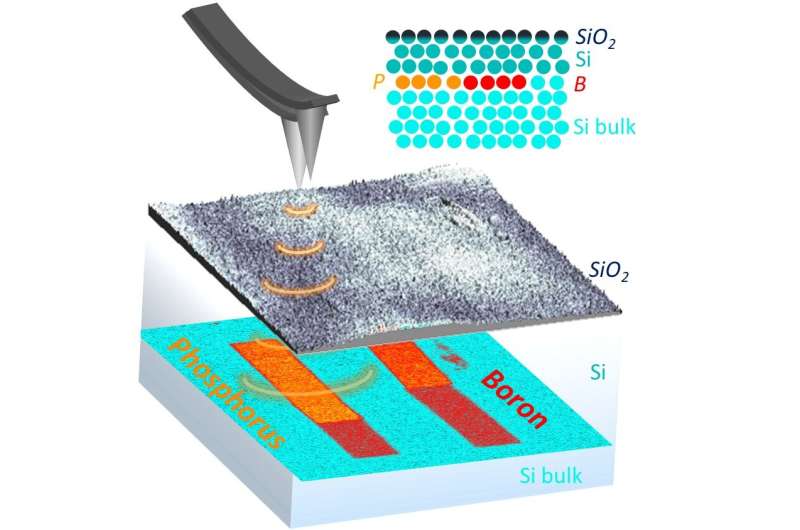
Credit: Gramse et al.
When fabricating integrated circuits and different types of silicon-based devices, researchers need to position dopant nanostructures in specific ways with high levels of precision. However, arranging these structures at the nanometer scale can be challenging, as their small size makes them difficult to observe and closely examine. Incorrectly tampering with them can have detrimental effects, which can potentially compromise a device's overall functioning and security.
With this in mind, researchers at Johannes Kepler University (JKU), Keysight Technologies Labs, University College London (UCL), and IBM Research have recently set out to develop a nanoscale imaging technique that can be used to observe dopant nanostructures in silicon-based devices with high precision. The method they developed, presented in a paper published in Nature Electronics, is the result of several years of research, following a joint Marie Curie- EU project that kicked-off in 2016.
"At JKU and Keysight Technologies Labs I was working on the development of new nanoscale characterization techniques that can look at nanoscale electrical properties of small features below a material's surface," Georg Gramse, one of the researchers who carried out the study, told Phys.org. "The big question for us was: how small can we go or how deep into the surface can we look and still see dopants or other conducting features? The question from our collegues at London Center for Nanotechnology (LCN) and IBM that joined the team a bit later was exactly the opposite: Where are our dopant structures? Are they where they should be, and are they activated and conducting?"
The researchers at JKU and Keysight Technologies Labs developed methods that can create nano-patterns of atomically thin n-type (phosphorus) an p-type (boron) dopant layers in silicon, as well as their resulting p-n junctions. This was done in close collaboration with nanotechnology experts at UCL and IBM.
So far, researchers have not found a single technique capable of measuring the 3-D location and electrical characteristics of dopant nanostructures in silicon devices while also collecting information about the charge dynamics of carriers and trapped charges in their surroundings. To achieve this, Gramse and his colleagues used a technique called broadband electrostatic force microscopy. This method can collect images with a higher resolution than those collected using standard imaging techniques and it is also non-destructive, which means that it does not damage a device while collecting measurements.
"Our technique resolves laterally with 10 nm, even if a feature is buried 15 nm below the surface, and detects the capacitate signature of subsurface charges at frequencies between 1kHz and 10GHz," Gramse said. "One of the its disadvantages, shared by other nanoscale techniques, is that in order to give this high resolution it needs a clean and relatively flat surface."
Gramse and his colleagues were among the first to develop a technique that can successfully extract quantitative information about the depth and dopant profile of nanostructures in silicon devices. The method they used also allowed them to gather information about the dynamics of carriers and trapped charges around these structures. This information can ultimately help to determine whether there are any traps in the silicon device, which may obstruct the movement of dopants inside it.
"I see many possible fields of application for our technique," Gramse said. "We will now continue investigating functional doping device imaging. Looking at the dynamics of electrical processes at the nanoscale is also of high interest in electrochemistry and energy materials, thus this will be another topic to focus on in our future work."
More information: Georg Gramse et al. Nanoscale imaging of mobile carriers and trapped charges in delta doped silicon p–n junctions, Nature Electronics (2020). DOI: 10.1038/s41928-020-0450-8
Journal information: Nature Electronics
© 2020 Science X Network


