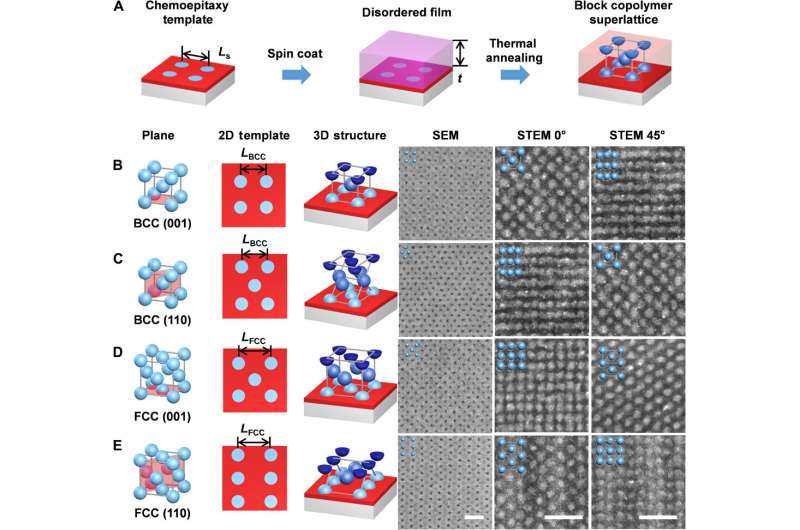
Controlling the symmetry and orientation of a BCP superlattice. (A) Schematic of the chemoepitaxy process flow. A 2D template is lithographically defined. A BCP is then spin coated onto the template. Thermal annealing enables DSA of the BCP into 3D superlattices. (B to E) Each row refers to the chemoepitaxy of three layers of PS-b-PMMA micelles on a specific template pattern: BCC (001), BCC (110), face-centered cubic (FCC) (001), and FCC (110). In each row from left to right, the panels correspond to the following: a unit cell showing the target plane, the 2D layout of the template matching the plane, the 3D structure of the lattice assembled on the template, top-down scanning electron microscopy (SEM) of the assembled sample, and STEM images of the assembled film taken at 0° and 45° sample tilt. For clarity, only the micelle cores are shown in the schematics. In the 3D structure of the assembled film, PMMA cores on different layers were colored in different shades of blue. The insets on the electron microscopy images show the expected structures. Scale bars, 100 nm. Credit: Science Advances, doi: 10.1126/sciadv.aaz0002
Three-dimensional (3-D) structures at the nanoscale are important in modern devices, although their fabrication with traditional top-down approaches is complex and expensive. Block copolymers (BCPs) that are analogous to atomic lattices can spontaneously form a rich variety of 3-D nanostructures to substantially simplify 3-D nanofabrication. In a new report on Science Advances, Jiaxing Ren and a research team in molecular engineering, chemical engineering and materials science at the University of Chicago, Technion-Israel Institute of Technology and the Argonne National Laboratory in the U.S. and Israel formed a 3-D superlattice using BCP micelles. They controlled the process using lithographically defined 2-D templates that matched a crystallographic plane in the 3-D superlattice. Using scanning transmission electron microscopy tomography, the team demonstrated precise control across the lattice symmetry and orientation. They achieved excellent ordering and substrate registration through 284-nanometer-thick films. To mediate lattice stability, the scientists tapped into molecular packing frustration of the superlattice and observed surface-induced lattice reconstruction, which led to form a unique honeycomb lattice.
A central challenge in materials science is to predict and control a crystallographic lattice built on atoms and molecules. In atomic epitaxy (a type of crystal growth), the underlying substrate can determine the lattice parameter and orientation of epitaxial growth. Precisely controlling lattice geometry of the epitaxial thin film can therefore offer scientists the opportunity to create structures with unique electronic, optoelectronic and magnetic properties. For example, in a simple case of A-B di-block copolymers, the chemically distinct A and B copolymers are covalently bound to form a macromolecule. They can separate and self-assemble into a range of shapes, such as cylinders and spheres depending on the block chemistries and volume fractions. Since such behaviors are typical in metallic alloys, the results suggest fundamental analogies between the mechanisms governing lattice stability in both hard and soft matter. Self-assembled structures in BCP thin films are directed and controlled by substrate templates with topographical features such as graphoepitaxy or chemical contrast known as chemoepitaxy.
Controlling the symmetry and orientation of a BCP superlattice.
Process flow for chemoepitaxy directed self-assembly of a sphere-forming block copolymer. (A) An 8-nm-thick cross-linkable polystyrene (X-PS) layer was coated and grafted onto the Si substrate. (B) A 40-nm-thick resist was coated and patterned with e-beam lithography. The film was then treated with O2 plasma to modify the wetting behavior of the exposed area. (C) The resist was removed to reveal the chemical template. (D) The block copolymer (BCP) was spin coated to a desired thickness. (E) The BCP was annealed at 190 °C to assemble into the superlattices of spherical micelles. Credit: Science Advances, doi: 10.1126/sciadv.aaz0002
During chemoepitaxy, a thin polymer layer can be lithographically defined and chemically modified to form a 2-D guiding template to preferentially interact with one of the blocks. The BCPs (block copolymers) are then coated onto the template to self-organize into highly ordered structures that comply with the lithographic pattern. Thus far scientists have incorporated directed self-assembly (DSA) of BCPs to perfect 2-D patterns in thin films and used them as etch masks for semiconductor fabrication. There is, however, tremendous untapped potential to directly form 3-D structures with perfect ordering and substrate registration based on BCP epitaxy to greatly simplify the process of 3-D nanofabrication. Ren et al. extended the ideas of DSA (directed self-assembly) to explore the design rules for 3-D BCP epitaxy, using a sphere-forming BCP as a model system. They used lithographically defined 2-D chemical templates during the process and varied the 2-D template designs and film thicknesses to examine lattice stabilities under a variety of strains, while noting the ability of epitaxy (crystal growth) to propagate through thick films. The epitaxy of the 3-D superlattice formed with BCP micelles provided guidance on epitaxy of more complex structures. The work offers new insight into fundamental mechanisms that govern symmetry control in soft and hard materials.
Ren et al. first showed control of the symmetry and orientation of the BCP superlattice using chemoepitaxy. They included polystyrene-block-poly(methyl methacrylate) (PS-b-PMMA) to form micelles containing a core made of the shorter PMMA block, while surrounded by a corona (head) made of the PS block. The micelles were spherical in shape in isolation, while forming space-filling polyhedra in the bulk polymer melt, to adopt a body-centered cubic (BCC) lattice. The scientists determined the shape of the bulk BCC lattice using small angle X-ray scattering. They then constructed a 3-D structure and used the back-etch method to confirm the conformation by preparing samples on a silicon nitride membrane for scanning transmission electron microscopy (STEM) characterization. Since lattice control in the study was based on manipulating the boundary conditions, the team observed polytypism (a variant of polymorphism) when different lattice structures shared the same layout and spacing on a plane.
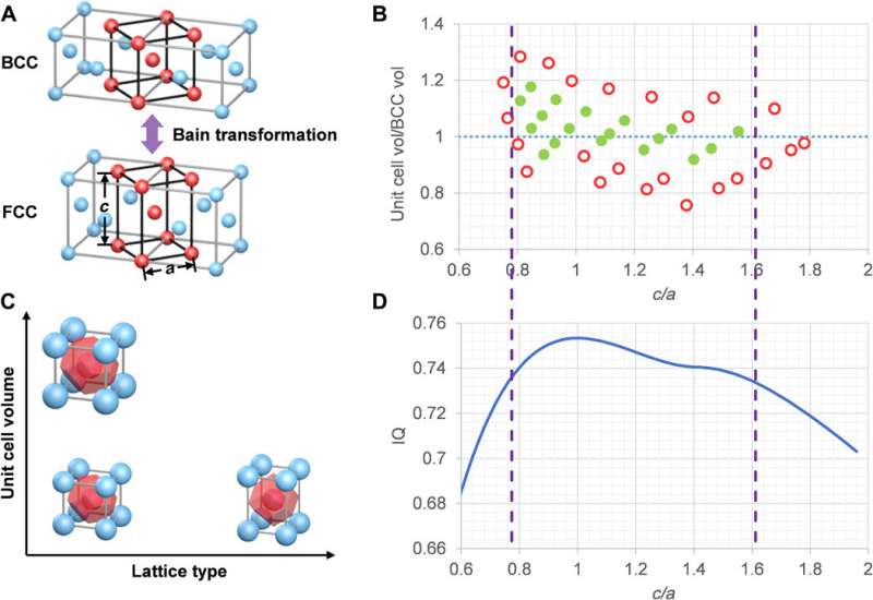
Bain transformation with 3D DSA. (A) BCC and FCC lattices can be connected through Bain transformation. The black lines and red spheres mark the BCT unit cell used to describe this transformation. Sphere diameter is reduced by half for clarity. (B) Process window of pseudomorphic epitaxy as shown by normalized unit cell volume versus lattice type. Green full circles represent well-ordered assembly, and red open circles represent films with terracing or random ordering. Blue dotted line signifies the same unit cell volume as that of the bulk BCC. (C) Schematics of the BCT unit cells and corresponding Wigner-Seitz cells (red polyhedron) in (B) showing the change in lattice type in the x direction and the change in unit cell volume in the y direction. (D) Sphericity of the Wigner-Seitz cells for different lattice symmetries as measured by the isoperimetric quotient (IQ). The purple dashed lines represent the boundary of the process window in (B). Credit: Science Advances, doi: 10.1126/sciadv.aaz0002
Lattice stability under strain and epitaxy through thick films
The scientists next investigated the lattice stability under biaxial tensile and compressive strains, where the resulting structures contained three layers of micelles to represent a body-centered tetragonal (BCT) symmetry. The outcome of tetragonal distortion in the study, connected the BCC (body-centered cubic lattice) with a face-centered cubic (FCC) lattice framework in a process referred to as Bain transformation. The resulting change in lattice type and unit cell volume correlated with changes in shape and volume of individual micelles. The scientists visualized the space occupied by each PS-b-PMMA micelle using Wigner-Seitz cells (a primitive unit cell).
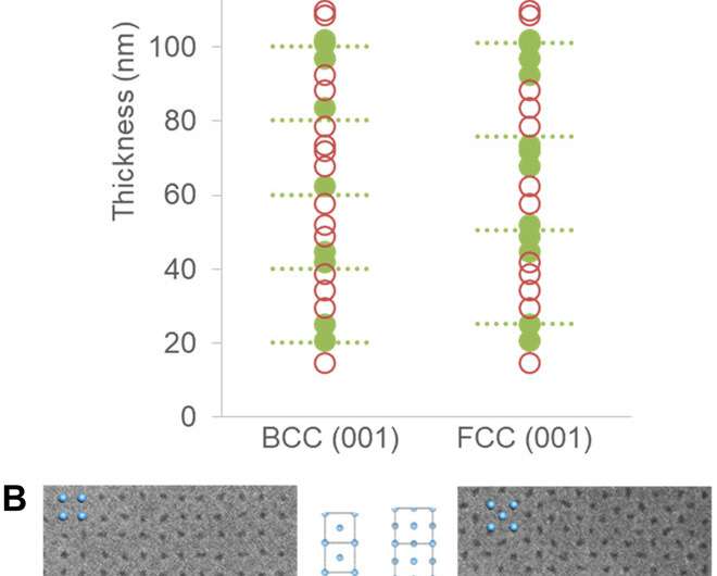
The work indicated the volumes of the micelles to be constant, validating previous assumptions used to design guiding templates for non-bulk lattices. The team maintained constant micelle volumes to avoid entropic penalties that could be triggered due to thickness of the film and the guiding template. The ultimate shape of self-assembled micelles resulted from balancing the need to fill a space uniformly and a tendency toward spherical symmetry in the setup. The team further investigated epitaxy (crystal growth) through thick films and studied the ability of the template pattern to propagate in the vertical direction.
DSA through thick films. (A) DSA on BCC (001) and FCC (001) templates with different film thicknesses. Well-ordered structures (filled green dots) were only achieved when film thickness was commensurate with the corresponding layer spacing (green dotted lines). (B) Top-down SEM images of DSA in 283.9-nm-thick film. Scale bars, 100 nm. Credit: Science Advances, doi: 10.1126/sciadv.aaz0002
Surface-induced lattice reconstruction
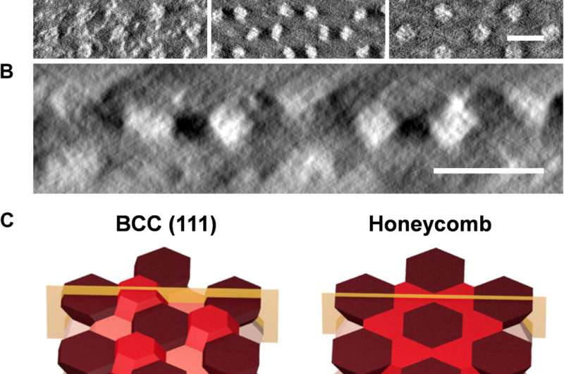
During additional studies, Ren et al. used STEM tomography to reveal a thin film containing three layers of micelles, where a center layer resembled a honeycomb pattern sandwiched between two layers of hexagonal half-micelles at the top and bottom. Using a digitally sliced cross-section, they showed the PMMA cores of micelles on the top and bottom layers to be centered in the six-member rings of the honeycomb layer. When they compared the unique honeycomb lattice to the body-centered cubic (BCC) lattice with four layers of micelles, the top and bottom layers appeared to be similar for both lattices, while the middle layer of the BCC lattice appeared to "merge" into one layer inside the honeycomb lattice. Using Wigner-Seitz cells, the team visualized the preference for the honeycomb lattice structure compared to the BCC lattice structure in the system—and credited the phenomenon as an attempt to avoid entropic penalties from chain stretching at the surface.
Formation of honeycomb lattice through lattice distortion. (A) In-plane slices created from STEM tomography showing the hexagonal symmetries at the top and bottom layers and the honeycomb symmetry in the middle layer. (B) Digitally sliced cross-section along the golden dashed line in (A) showing the three-layer honeycomb lattice. (C) 3D schematics of BCC (111) and honeycomb lattice showing the arrangements of the Wigner-Seitz cells. Cells at different layers are colored with different shades of red. (D) Cross-section along the golden plane in (C) showing the uneven surfaces of BCC (111) versus the flat surfaces of honeycomb lattice. Scale bars, 50 nm. Credit: Science Advances, doi: 10.1126/sciadv.aaz0002
In this way, Jiaxing Ren and colleagues demonstrated a set of design rules for the 3-D assembly of BCP micelles using 2-D templates. They precisely controlled the crystallographic symmetries and orientations based on template design and film thicknesses. The highly ordered, tailorable superlattices can be incorporated into photonic and plasmonic material design. The team can functionalize the micelles by tuning the polymer chemistry, or by converting the assembled structures to metal or metal oxides. The results also showed intriguing analogies between BCP epitaxy and atomic epitaxy. The lithographically defined templates in this work offered flexibility to decipher fundamental principles of symmetry control.
More information: Jiaxing Ren et al. Three-dimensional superlattice engineering with block copolymer epitaxy, Science Advances (2020). DOI: 10.1126/sciadv.aaz0002
N. SELJAKOW. The Nature of Martensite, Nature (2008). DOI: 10.1038/123204a0
Jinan Chai et al. Assembly of aligned linear metallic patterns on silicon, Nature Nanotechnology (2007). DOI: 10.1038/nnano.2007.227
Journal information: Science Advances , Nature , Nature Nanotechnology
© 2020 Science X Network


