Novel tin 'bubbles' spur advances in the development of integrated chips

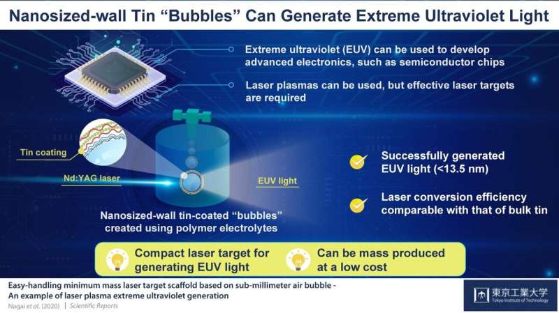
The use of extreme ultraviolet light sources in making advanced integrated chips has been considered, but their development has been hindered owing to a paucity of efficient laser targets. Scientists at Tokyo Institute of Technology (Tokyo Tech) recently developed an extremely low-density tin 'bubble,' which makes the generation of extreme ultraviolet reliable and low cost. This novel technology paves the way for various applications in electronics and shows potential in biotechnology and cancer therapy.
Development of next-generation devices requires that their core, called the integrated circuit chip, is more compact and efficient than existing ones. Manufacturing these chips requires powerful light sources. The use of light sources in the extreme ultraviolet (EUV) range (an extremely short-wavelength radiation) has become popular in recent times, but their generation is challenging.
One solution is the use of high-intensity lasers: Recent advances in laser technology have led to the development of lasers with increased power and lower prices. High-intensity lasers implement laser plasmas, and their first practical application is the generation of EUV light to manufacture semiconductor integrated circuits. In this process, these lasers irradiate an appropriate 'target,' and as a result, a high-temperature and high-density state is created. From this state, 13.5 nm light is generated with high brightness, which can be used in the manufacturing of integrated chips. But this is not an easy feat: control of target density that can produce light in the EUV range has been difficult. Tin has been considered as an option, but its development has been greatly delayed owing to the inability to control its dynamics.
To this end, a team of scientists, including Associate Professor Keiji Nagai from Tokyo Tech and Assistant Professor Christopher Musgrave from University College, Dublin, set out to find efficient laser targets. In a study published in Scientific Reports, they describe a novel type of low-density material, which is scalable and low-cost. Prof Nagai says, "EUV light has become crucial in today's world but is expensive owing to the high-volume manufacturing."
To begin with, the scientists created a tin-coated microcapsule or 'bubble,' a very low-density structure—weighing as little as 4.2 nanogram. For this, they used polymer electrolytes (dissolution of salts in a polymer matrix), which act as surfactants to stabilize the bubbles. The bubbles were then coated with tin nanoparticles. Prof Nagai explains, "We produced polyelectrolyte microcapsules composed of poly(sodium 4-styrene-sulfonate) and poly(allylamine hydrochloride) and then coated them in a tin oxide nanoparticle solution."
To test the use of this bubble, the scientists irradiated it using a neodymium-YAG laser. This, indeed, resulted in the generation of EUV light, which is within the 13.5 nm range. In fact, the scientists even found that the structure was compatible with conventional EUV light sources that are used to manufacture semiconductor chips. But, the biggest advantage was that the laser conversion efficiency with the tin bubble, a measure of the laser power, matched that of bulk tin. Prof Nagai explains, "Overcoming the limitations of liquid tin dynamics can be very advantageous in generating EUV light. Well-defined low-density tin targets can support a wide range of materials including their shape, pore size, density etc."
Prof Nagai and his research team have been developing low-density materials for laser targets for many years but had been suffering limitations with manufacturing costs and mass productivity. Now, combining new low-density tin targets made of bubbles offers an elegant solution for mass producing a compact 13.5 nm light source at a low cost. In addition to its applications in electronics, Prof Nagai is optimistic that their novel technology consisting of "bubble" laser targets could even be used in cancer therapy. He concludes, "This method could be utilized as a potential small scale/compact EUV source, and future quantum beam sources such as electrons, ions, and X-rays by changing the coating to other elements." Through this opportunity, Prof Nagai and his team wish to collaborate with large laser facilities in Japan and overseas.
More information: Christopher S. A. Musgrave et al, Easy-handling minimum mass laser target scaffold based on sub-millimeter air bubble -An example of laser plasma extreme ultraviolet generation-, Scientific Reports (2020). DOI: 10.1038/s41598-020-62858-3
Journal information: Scientific Reports
Provided by Tokyo Institute of Technology


