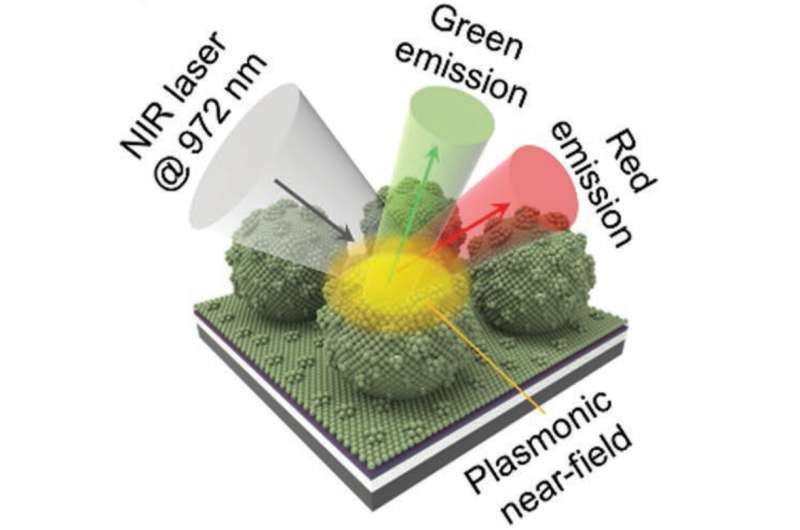
The 3D conceptual illustration of the luminescent film. Credit: Korea Institute of Science and Technology (KIST)
Infrared radiation, which is invisible yet highly utilizable, is used in various fields and for various purposes, such as for coronavirus detection (i.e. through thermal imaging cameras and biosensors). A Korean research team has developed a technology that visualizes infrared radiation and expands its application range.
The Korea Institute of Science and Technology (KIST, Acting President Yoon Seok-jin) announced that Dr. Kwon Seok-joon's research team at the Nanophotonics Research Center has developed a multi-functional luminescent film that can visualize near-infrared light through wavelength conversion that converts near-infrared light to visible light. The research was jointly conducted by the KIST team and Ko Doo-hyun, a professor of applied chemistry at Kyung Hee University (President Han Gyun-tae).
The conversion of invisible infrared or ultraviolet light into visible light allows us to intuitively see the data contained in the light, and thus enables the use of infrared or ultraviolet light for displays or imaging devices. Quantum dots, recently used for high-definition TVs, can be seen as a type of wavelength conversion technology that converts ultraviolet light into visible light in displays.
Ultraviolet light is high in energy, which makes its conversion into visible light relatively easy and enables high conversion efficiency. In contrast, near-infrared light is low in energy, and at least two near-infrared photons are absorbed and converted into one higher-energy photon. The conversion efficiency of converting near-infrared light into visible light is extremely low and is about 1/100 to 1/1000 the efficiency of converting quantum dots into visible light. This was a major stumbling block in making the near-infrared-to-visible light conversion more realistic for wider applications in various fields in the form of sensors, displays, and imaging devices.
The research team at KIST made a square lattice array of oxidized silicon (silica) microbeads decorated with up-conversion nanoparticles and metal structures. This configuration maximizes both the absorption of near-infrared light and the luminescence of visible light, thus increasing the efficiency of near-infrared-to-visible light conversion by nearly 1,000 times.
The lattice configuration of silica microbeads developed by the research team can easily be transferred to a transparent film. This type of film was found to be flexible, foldable, and even washable with the light intensity maintained after wavelength conversion.
"Existing infrared sensors can only collect one type of data, but this technology can be used to collect various types of data all at once and visualize them," said Dr. Kwon Seok-joon from KIST, who led the research. "Since this technology has various advantages in processing, such as foldability, washability, and transferability into other films, its application can be extended throughout various fields, and it can be used for foldable devices, wearable sensors, and flexible wavelength conversion imaging devices."
More information: In‐Hwan Ahn et al, A Multi‐Functional Highly Efficient Upconversion Luminescent Film with an Array of Dielectric Microbeads Decorated with Metal Nanoparticles, Advanced Functional Materials (2020). DOI: 10.1002/adfm.201909445
Journal information: Advanced Functional Materials
Provided by National Research Council of Science & Technology


