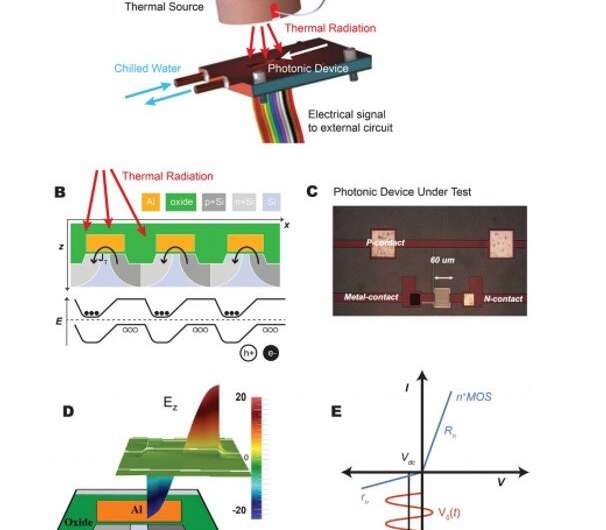
Grating-coupled bipolar tunnel diode thermal photovoltaic device. (A) Illustration of thermal illumination of bipolar thermal photovoltaic device in vacuum radiometry setup. Device is packaged and mounted of a chilled stage with temperature stabilized at 20°C. (B) Schematic of multiple periods of bipolar thermal photovoltaic device illustrating the charge pumping mechanism. (C) Image of actual bipolar grating coupled tunnel diode at resonance with front side contacting scheme. (Grating area is 60 μm × 60 μm.) (D) The modeled transverse spatial field profile in thin tunnel barrier at peak field confinement. This confined field leads to the driven photon-assisted tunneling. (E) The model IV tunneling characteristic for the n+ MOS tunnel diode. Rn and rn are the diode resistances in forward and reverse bias and the rectification of the tunneling current. (Model p+ MOS leads to similar IV characteristics.) Credit: Science Advances, doi: 10.1126/science.aba2089
Moderate-temperature thermal sources often radiate waste heat as a by-product of mechanical work, chemical or nuclear reactions, or information processing. In a new report in Science, Paul S. Davids and a research team at the Sandia National Laboratory in the U.S., demonstrated the conversion of thermal radiation into electrical power. For this, they used a bipolar grating-coupled complimentary metal-oxide-silicon (CMOS) tunnel diode. Using a two-step photon-assisted tunneling charge pumping mechanism, the team separated the charge carriers in pn junction wells to develop a large, open-circuit voltage across a load. The scientists experimentally showed electrical power generation from a broadband blackbody thermal source with converted power densities of 27 to 61 µW/cm2 for thermal sources between 250 degrees C to 400 degrees C. The demonstrated scalable and efficient conversion of radiated waste heat into electrical power can be used to reduce energy consumption—in order to power electronics and sensors.
At finite temperature—all objects radiate due to thermal fluctuations of their atomic constituents in a characteristic spectrum that depends on the surface temperature and spectral emissivity of the object. The sun's radiative heat transfer is the dominant radiative energy resource currently available to Earth and photovoltaic power generation is an effective and rapidly growing technique aiming to convert this incident radiation to electrical power (e.g. solar cells). However, other sources of radiative heat including cooler terrestrial sources or man-made waste heat can give rise to considerable net energy exchange as a readily available electrical power source, provided efficient conversion.
New approaches for energy conversion and photon-mediated charge pumping.
Thermophotovoltaic (TPV) devices that convert radiation from broadband thermal sources into electrical power are promising technologies to convert solar energy and for waste heat recovery. Such devices generally work by heating a secondary thermal source as a selective emitter, where an emission spectrum is filtered and matched to a small bandgap semiconductor device. The semiconductor device can be pn junction designed for absorption of a photon to take place in its depletion region creating an electron hole pair and result in the separation of charge and the induction of an open-circuit voltage across the device. However, TPV conversion from a moderate temperature source for large-scale power generation can be very challenging. Scientists have therefore proposed a variety of approaches for improved TPV conversion efficiency from moderate temperature sources.
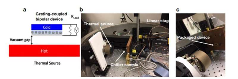
Vacuum thermal photovoltaic measurement system (a) Schematic device configuration for thermal to electrical power conversion. RLoad is a variable load resistance outside of vacuum. (b) Circular heater coated with blackbody high emissivity paint used for thermal source. Sample is on chilled copper block mounted on a linear stage for position control. (c) Packaged sample is flush mounted and electrically contacted from the backside with thermocouples mounted to front of sample and backside of sample package for temperature monitoring. Credit: Science Advances, doi: 10.1126/science.aba2089
For example, alternative approaches for thermal to electrical conversion were based on direct rectification (converting alternative current to direct current) of infrared radiation using ultra-fast tunneling. Davids et al. suggested a new means for thermal photovoltaic conversion from a low-grade thermal source in the temperature range of 100 degrees C to 400 degrees C via photon-assisted tunneling and a spatially-varying confined optical field in the tunnel barrier. An interdigitated bipolar pn junction array under the tunneling gate electrode acted as a charge pump to move electrons from the p-type region to the n-type region within the optical field. The scientists optimized the setup and contacted the interdigitated p and n regions separately to measure power generation across a variable external load resistance, R—which shorts the pn junction. The effective diode voltage multiplier circuits resulted in orders of magnitude improvement in electrical power generation compared to direct rectification.
Modelling the device.
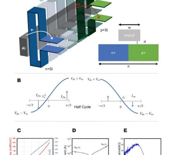
Bipolar grating-coupled tunnel diode model. (A) Equilibrium band diagram of bipolar device under metal gate showing electron and hole particle currents. (Inset shows unit cell geometry. The period of the grating is P = 3 μm, the metal width is w = 1.8 μm, and d = 3–4.5 nm.) (B) The instantaneous voltage profile in the device at t = 0 and at t = T/2. The spatially varying currents occur in both n and p+ regions and the voltage node shifts to negative x position. The half period instantaneous voltage profile and currents across the device. The voltage node shifts to positive x position. (C) Integrated blackbody source power per unit area (red curve) for bandwidth between c/8.0 μm to c/7.0 μm with field enhancement γ = 20, and d = 4 nm. Blue curve is associated AC voltage amplitude Vm. (D) Measured tunnel diode characteristic for typical n+ MOS tunnel diode with resonant PAT single photon voltage marked. (E) Extracted resistance from n+ MOS tunnel diode. Rn ≃ 200 Ω and rn ≃ 50,000 Ω at the indicated photovoltages. Credit: Science Advances, doi: 10.1126/science.aba2089
An ideal device model for thermal photovoltaic conversion in a bipolar antenna-coupled tunnel diode rectifier generally contains a buried symmetric pn junction, under an equilibrium MOS (metal-oxide-silicon) metal gate. The device can be illuminated by a thermal source modelled as a blackbody broadband emitter. Davids et al. observed a complex current due to the complex admittance (current flow) of the tunnel diode, based on its conductance and capacitance. The self-consistent dc voltage could be estimated by the current-matching condition, which required the half-cycle currents generated in the device to be equal and in opposite directions. As a key feature of the bipolar conversion device, the team noted a periodic buried pn junction under the metal, for charge storage, pumped by the combined action of the two forward biased tunnel junctions. They noted that larger the open circuit voltage, greater the power generation in the bipolar device.
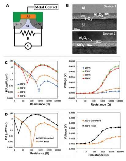
Bipolar device power generation. (A) Circuit schematic of device contacts for power generation. (B) TEM cross-sections through nominal 4 nm gate oxide stack (Device 1) and through nominal 3.5 nm gate oxide stack (Device 2). (C) Measured power density for device 1 as a function of the load resistance for various source temperatures and measured voltage across pn junction shorted by a load resistor versus load resistance for various source temperatures. (D) Measured power density for device 2 as a function of the load resistance at fixed source temperature for grounded and floating metal gate and measured voltage across pn junction shorted by a load resistor versus load resistance. Credit: Science Advances, doi: 10.1126/science.aba2089
Experimental results
The scientists measured electrical power generation from a moderate temperature source using a vacuum TPV setup, with an approximate 2-mm scale gap between the sample and the heat source. The device contained three-terminals with interdigitated n and p regions with separate n, p and metal contacts. They measured the induced voltage from the thermal source at fixed temperature by shorting the pn junctions with a variable load resistor. They followed this with measurements of the induced voltage as a function of the load resistance with a nanovoltmeter. The process and device parameters played an integral role during the performance of the bipolar device.
The oxide thickness and composition of the device also affected the tunneling resistance and epsilon-near-zero dispersion field concentration. In addition, the implant conditions and thermal annealing cycles greatly affected the pn junction characteristics under the metal gate. Davids et al. confirmed the features of the fabricated devices using two transmission electron microscope (TEM) cross-sectional images, of two different devices (device 1 and device 2) – taken beneath the gate metal.
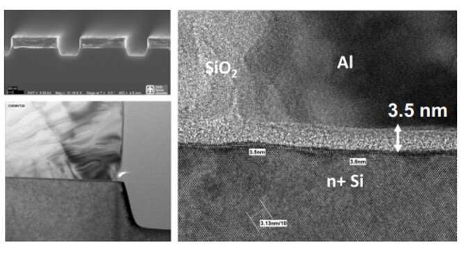
SEM and TEM of infrared grating coupled MOS tunnel diode Unipolar grating coupled tunnel diode with back-side contact. The bipolar grating coupled device has front-side contact and hence thin-alumina in tunnel diode stack. Credit: Science Advances, doi: 10.1126/science.aba2089
Davids et al. confirmed alumina makeup of the devices using energy dispersive X-ray spectroscopy (EDS). The impact of the thick alumina layer shifted the peak power density to lower source temperatures, since longitudinal phonon resonances occurred approximately at 200 degrees C. The work showed a complex interaction of the gate oxide longitudinal phonon mode and device design parameters that determined the output power for this new form of photovoltaic conversion. This allowed Davids et al. to adjust the operational temperature of the device by tuning the longitudinal phonon resonance. The bipolar devices far exceeded the limit of direct rectification (ac to dc conversion), suggesting that photon-assisted tunneling and charge separation could be further improved through device and process optimization.
In this way, Paul S. Davids and colleagues demonstrated efficient conversion of moderate-temperature radiative thermal sources as a largely untapped resource for energy harvesting. They built radiative thermal to electrical energy conversion on a bipolar grating-coupled tunneling device as a scalable, compact energy harvesting technology. The devices can be used as a stand-alone energy converter or in conjunction with thermoelectric power generators. The method relies on n- and p-type wells in a bipolar grating-coupled device. The results showed an electrical power density of 61 µW/cm2 from a 350 degrees C thermal source for an estimated conversion efficiency approaching the efficiency of TPV conversion—but with significantly cooler source temperatures. Davids et al. will optimize the device architecture and its process for improved power generation.
More information: Paul S. Davids et al. Electrical power generation from moderate-temperature radiative thermal sources, Science (2020). DOI: 10.1126/science.aba2089
W. R. Chan et al. Toward high-energy-density, high-efficiency, and moderate-temperature chip-scale thermophotovoltaics, Proceedings of the National Academy of Sciences (2013). DOI: 10.1073/pnas.1301004110
Anthony Fiorino et al. Nanogap near-field thermophotovoltaics, Nature Nanotechnology (2018). DOI: 10.1038/s41565-018-0172-5
Journal information: Science , Proceedings of the National Academy of Sciences , Nature Nanotechnology
© 2020 Science X Network
