January 13, 2020 feature
Hyperuniform disordered waveguides and devices for near infrared silicon photonics
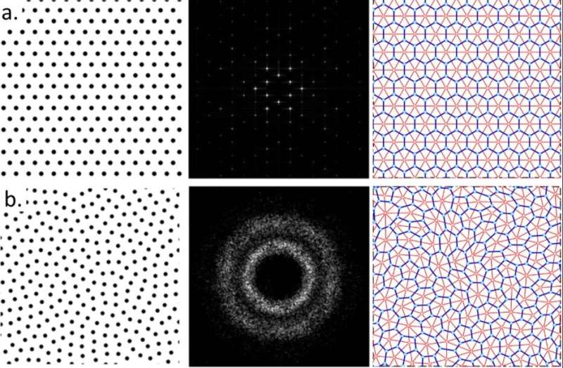
In a new report published on Scientific Reports, Milan M. Milošević and an international research team at the Zepler Institute for Photonics and Nanoelectronics, Etaphase Incorporated and the Departments of Chemistry, Physics and Astronomy, in the U.S. and the U.K. Introduced a hyperuniform-disordered platform to realize near-infrared (NIR) photonic devices to create, detect and manipulate light. They built the device on a silicon-on-insulator (SOI) platform to demonstrate the functionality of the structures in a flexible, silicon-integrated circuit unconstrained by crystalline symmetries. The scientists reported results for passive device elements, including waveguides and resonators seamlessly integrated with conventional silicon-on-insulator strip waveguides and vertical couplers. The hyperuniform-disordered platform improved compactness and enhanced energy efficiency as well as temperature stability, compared to silicon photonic devices fabricated on rib and strip waveguides.
Academic and commercial efforts worldwide in the field of silicon photonics have led to engineer optical data communications at the Terabit-scale at increasingly lower costs to meet the rapidly growing demand in data centers. Explosive growth in cloud computing and entertainment-on-demand pose increasingly challenging costs and energy requirements for data transmission, processing and storage. Optical interconnects can replace traditional copper-based solutions to offer steadily increasing potential to minimize latency and power consumption, while maximizing the bandwidth and reliability of the devices. Silicon photonics also leverage large-scale, complementary metal-oxide semiconductor (CMOS) manufacturing processes to produce high-performance optical transceivers with high yield at low-cost. The properties allow applications of optical transceivers (fiber optical technology to send and receive data) to be increasingly compelling across shorter distances.
More than three decades ago, physicist Richard Soref identified silicon as a promising material for photonic integration. Leading to the present-day steady development and rapid production of increasingly complex photonic integrated circuits (PICs). Researchers can integrate large numbers of massively-parallel compact energy-efficient optical components on a single chip for cloud computing applications from deep learning to artificial intelligence and the internet of things. Compared to the limited scope of commercial silicon photonic systems, photonic crystal (PhC) architectures promise smaller device sizes, although they are withheld by layout constraints imposed by waveguide requirements along the photonic crystal's axis. Until recently, photonic band gap (PBG) structures that efficiently guide light were limited to photonic crystal platforms. Now, newer classes of PBG structures include photonic quasicrystals, hyperuniform disordered solids (HUDs) and local self-uniform structures.
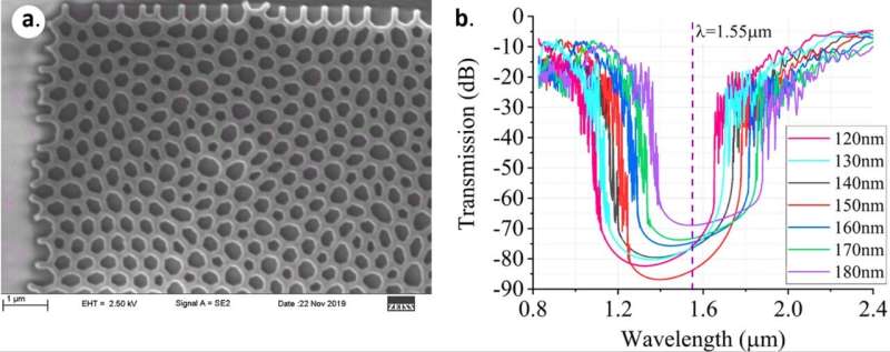
In the present work, Milošević et al. introduced a HUD (hyperuniform disordered solid) platform as a locally engineered photonic system and generic architecture for photonic integrated circuits. They demonstrated the HUD platform's design flexibility and built-in ability for seamless integration into pre-designed optical cavities and waveguides. The silicon-on-insulator (SOI) HUDs have great potential in a host of applications at optical communication wavelengths. Compared to standard micro-ring resonators (MRRs) or Mach-Zehnder interferometers (MZIs), HUD resonators exhibited less temperature-dependent resonant wavelength shift (TDRWS) and increased compactness. The results revealed promising prospects for device improvement and lower power consumption.
The team first obtained a scanning electron micrograph (SEM) image of a HUD network fabricated using electron-beam lithography on a 220-nm high, SOI wafer. Followed by finite difference time-domain simulations of the transmission spectrum for transmission electric polarized light through hyperuniform networks with an average separation of 500 nm and various wall widths. Milošević et al. tuned the central wavelength of these bandgaps by modifying the wall width of the HUDs and the wide bandgaps allowed them to cover a wavelength range of 1.50 to 1.58 micrometers (µm) for the networks to be well-suited for photonic circuit design.
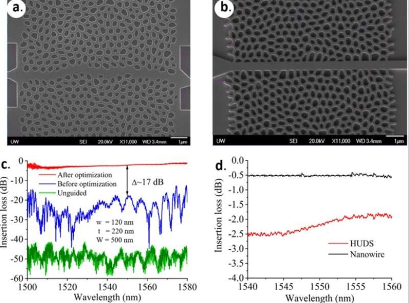
The scientists designed and developed waveguides as a series of in-line defects by substituting one row of polygon-shaped air cells along desired paths with filled silicon. The SEM images of fabricated SOI HUD waveguides allowed a variety of optimization approaches to increase transmission through the waveguide channel. To minimize backscattering losses, they optimized the waveguide structure via one-step optimization, which substantially reduced the initial high backscattering loss. The team observed the transmission spectrum through HUD waveguides before and after optimization and transmission in the absence of the waveguide channel to experimentally verify a 17 dB improvement at around 1550 nm.
The HUD platform supported a rich set of new resonator designs including resonant cavities with symmetries unavailable in photonic crystal structures. The HUD platform was also versatile and flexible for new types of cavities and waveguide designs allowing seamless integration in state-of-the-art designs, while maintaining a very high quality (Q) factor (signal quality of an optical channel). The approach advantageously allowed any device to be integrated with minimal effort on the same platform with freeform HUDsian cladding, provided the researchers arranged appropriate insulation of the various components. Based on simulations, they found the HUD device footprint to be small but the Q factor to remain large.
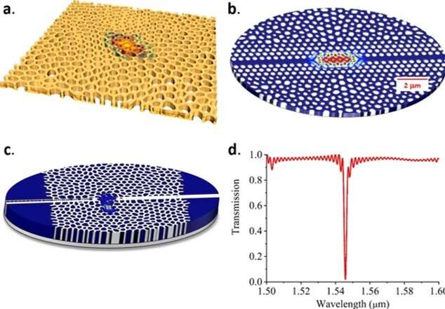
Milošević et al. next investigated an electrically-controlled optical modulator featuring an air-bridged resonant cavity in a HUDS structure. The team mainly aimed to demonstrate the versatility of the HUD platform to integrate a variety of optical components while maintaining their state-of-the-art performance. They recorded both electron distribution density and the local refractive index as a function of the bias voltages within the setup. The research team easily tuned the electron distribution density and local refractive index by applying small voltages.
They then applied a forward bias (flow of larger current in one direction) to the setup to demonstrate the transmittance spectrum shift toward a shorter wavelength. The results implied the reduced refractive index of silicon as expected for the plasma dispersion effect. The scientists predicted 0.48 V to be the threshold voltage to operate a modulator at a 10 dB on/off ratio and observed low power operation due to the small size and high Q of the resonant cavity.
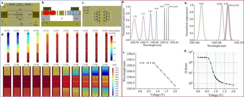
In this way, Milan M. Milošević and colleagues demonstrated experimental and simulation results of HUD (hyperuniform disordered solid)-integrated devices to explore HUD functionality as a flexible and compact platform for photonic integrated circuits. They improved the device fabrication process to reduce propagation losses and optimized the transition between the HUDs and strip waveguides using wider waveguides and treatment post-fabrication. The scientists employed the HUDs to facilitate light confinement in predefined PhC (photonic crystal) resonant cavities and enhance their temperature stability.
The intrinsic isotropy (uniformity in all orientations) of the new disordered PBG (photonic band gap) materials demonstrated potential for photonic device design by offering compactness, low-power consumption and improved temperature stability. The devices also offered unprecedented design freedom without limitations by crystalline structures or periodicity. The disordered materials character made them less sensitive to fabrication errors, compared to their periodic counterparts. The HUD-based resonant devices demonstrated a clear ability to guide and localize light in the infrared region with low-loss. The HUD devices provided new building blocks to design more complex systems featuring passive and active devices in semiconductor material platforms, for new opportunities in cost-effectively increased data rates and data storage.
More information: Milan M. Milošević et al. Hyperuniform disordered waveguides and devices for near infrared silicon photonics, Scientific Reports (2019). DOI: 10.1038/s41598-019-56692-5
Richard Soref. Mid-infrared photonics in silicon and germanium, Nature Photonics (2010). DOI: 10.1038/nphoton.2010.171
Weining Man et al. Experimental measurement of the photonic properties of icosahedral quasicrystals, Nature (2005). DOI: 10.1038/nature03977
Journal information: Scientific Reports , Nature Photonics , Nature
© 2020 Science X Network


