Semiconductors are the basic building blocks of digital devices. Improvements in semiconductor functionality and performance are likewise enabling next-generation applications of semiconductors for computing, sensing and energy conversion. Yet researchers have long struggled with limitations in their ability to fully understand the electronic charges inside semiconductor devices and advanced semiconductor materials, limiting researchers' ability to drive further advances.
In a new study in the journal Nature, an IBM Research-led collaboration describes an exciting breakthrough in a 140-year-old mystery in physics—one that enables researchers to unlock the physical characteristics of semiconductors in much greater detail and aid in the development of new and improved semiconductor materials.
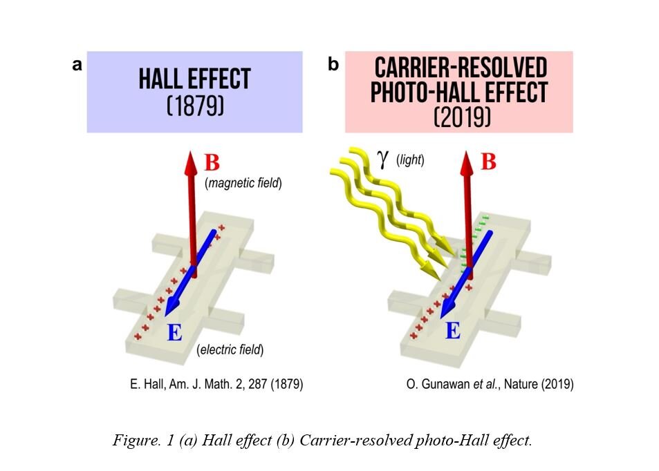
To truly understand the physics of semiconductors, we first need to know the fundamental properties of the charge carriers inside the materials, whether those particles are positive or negative, their speed under an applied electric field and how densely they are packed in the material. Physicist Edwin Hall found a way to determine those properties in 1879, when he discovered that a magnetic field will deflect the movement of electronic charges inside a conductor and that the amount of deflection can be measured as a voltage perpendicular to the flow of charge as shown in Fig. 1a. This voltage, known as the Hall voltage, unlocks essential information about the charge carriers in a semiconductor, including whether they are negative electrons or positive quasi-particles called "holes," how fast they move in an electric field or their "mobility" (µ) and their density (n) inside the semiconductor.
A 140-year-old secret
Decades after Hall's discovery, researchers also recognized that they can perform the Hall effect measurement with light—which are called photo-Hall experiments, as shown in Fig. 1b. In such experiments, the light illumination generates multiple carriers or electron hole pairs in the semiconductors. Unfortunately, the understanding of the basic Hall effect provided insights into only the dominant charge carrier (or majority carrier). The researchers were unable to extract the properties of both carriers (the majority and minority carriers) simultaneously. Such information is crucial for many applications that involve light such as solar cells and other optoelectronic devices.
IBM Research's study in Nature unlocks one of the Hall effect's long-held secret. Researchers from KAIST (Korea Advanced Institute of Science and Technology), KRICT (Korea Research Institute of Chemical Technology), Duke University, and IBM discovered a new formula and technique to extract the majority and minority carrier information such as density and mobility, as well as to gain additional insights about carrier lifetimes, diffusion lengths and the recombination process.
To be more specific, in the photo-Hall experiment, both carriers contribute to changes in conductivity (σ) and Hall coefficient (H, which is proportional to the ratio of the Hall voltage to the magnetic field). The key insight comes from measuring the conductivity and Hall coefficient as a function of light intensity. Hidden in the trajectory of the conductivity-Hall coefficient (σ-H) curve, reveals a crucial new information: the difference in mobility of both carriers. As discussed in the paper, this relationship can be expressed elegantly as: Δµ = d (σ²H)/dσ
Starting with a known majority carrier density from the traditional Hall measurement in the dark, the researchers solved for both majority and minority carrier mobility and density as a function of light intensity. The team named the new technique Carrier-Resolved Photo Hall (CRPH) measurement. With a known light illumination intensity, the carrier lifetime can similarly be established. This relationship and the related solutions have been hidden for nearly a century and a half, since the discovery of the Hall effect.
Beyond advances in this theoretical understanding, advances in experimental techniques are also critical to enabling this new technique. The technique requires a clean Hall signal measurement, which can be challenging for materials where the Hall signal is weak (e.g. due to low mobility) or when extra unwanted signals are present, such as under strong light illumination. For this purpose, one needs to perform the Hall measurement with an oscillating (ac) magnetic field. Like listening to radio, one must select the desired station's frequency while rejecting all other frequencies that act as noise. The CRPH technique goes a step further and selects not only the desired frequency, but also to the phase of the oscillating magnetic field in a technique called lock-in detection. This concept of AC Hall measurement has long been known, but the traditional technique using an electromagnetic coil system to generate the AC magnetic field was inefficient.
A precursor discovery
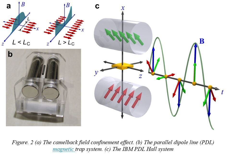
As often occurs in science, advances in one area are triggered by discoveries in another. In 2015, IBM Research reported a previously unknown phenomenon in physics related to a new magnetic field confinement effect, nicknamed the "camelback" effect, which occurs between two lines of transverse dipoles when they exceed a critical length as shown in Fig. 2a. The effect is a key feature that enables a new type of natural magnetic trap, called parallel dipole line (PDL) trap as shown in Fig. 2b. The PDL magnetic trap could serve as novel platform for various sensor applications such as a tiltmeter and seismometer (earthquake sensor). Such novel sensor systems together with big data technology could open many new applications and are being studied by the IBM Research team developing a big data analytics platform called IBM Physical Analytics Integrated Repository Service (PAIRS), which hosts myriad geospatial and Internet of Things (IoT) sensor data.
The same PDL element has another unique application. When rotated, it serves as an ideal system for a photo-Hall experiment to obtain strong, unidirectional and pure harmonic magnetic field oscillation (Fig 2c). More importantly, the system provides ample space to allow large area illumination onto the sample, which is critical in the photo-Hall experiment.
The impact
The newly developed photo-Hall technique extracts an astonishing amount of information from semiconductors. In contrast to only three parameters obtained in the classical Hall measurement, this new technique yields up to seven parameters at every tested light intensity. These include the mobility for both electron and hole; their carrier density under light; recombination lifetime; and diffusion lengths for electron, holes and ambipolar type. All of these can be repeated N times (i.e. the number of light intensity settings used in the experiment).
This new discovery and technology will help push semiconductor advances in both existing and emerging technologies. It provides the knowledge and tools needed to extract the physical characteristics of semiconductor materials in great detail. For example, this could accelerate development of next-generation semiconductor technology such as better solar cells, better optoelectronics devices and new materials and devices for artificial intelligence technology.
More information: Oki Gunawan et al. Carrier-resolved photo-Hall effect, Nature (2019). DOI: 10.1038/s41586-019-1632-2
E. H. Hall. On a New Action of the Magnet on Electric Currents, American Journal of Mathematics (2006). DOI: 10.2307/2369245
Journal information: Nature
Provided by IBM


