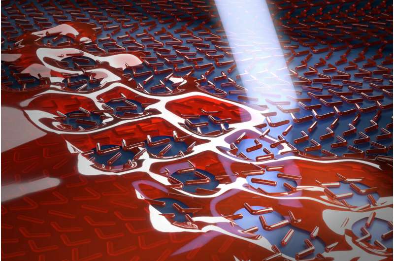
The new method employs a natural process already used in fluid mechanics: dewetting. Credit: © Vytautas Navikas / 2019 EPFL
Optical circuits are set to revolutionize the performance of many devices. Not only are they 10 to 100 times faster than electronic circuits, but they also consume a lot less power. Within these circuits, light waves are controlled by extremely thin surfaces called metasurfaces that concentrate the waves and guide them as needed. The metasurfaces contain regularly spaced nanoparticles that can modulate electromagnetic waves over sub-micrometer wavelength scales.
Metasurfaces could enable engineers to make flexible photonic circuits and ultra-thin optics for a host of applications, ranging from flexible tablet computers to solar panels with enhanced light-absorption characteristics. They could also be used to create flexible sensors for direct placement on a patient's skin, for example, in order to measure things like pulse and blood pressure or to detect specific chemical compounds.
The catch is that creating metasurfaces using the conventional method, lithography, is a fastidious process that takes several hours and must be done in a cleanroom. But EPFL engineers from the Laboratory of Photonic Materials and Fiber Devices (FIMAP) have now developed a simple method for making them in just a few minutes at low temperatures—or sometimes even at room temperature—with no need for a cleanroom. The EPFL's School of Engineering method produces dielectric glass metasurfaces that can be either rigid or flexible. The results of their research appear in Nature Nanotechnology.
Turning a weakness into a strength
The new method employs a natural process already used in fluid mechanics: dewetting. This occurs when a thin film of material is deposited on a substrate and then heated. The heat causes the film to retract and break apart into tiny nanoparticles. "Dewetting is seen as a problem in manufacturing—but we decided to use it to our advantage," says Fabien Sorin, the study's lead author and the head of FIMAP.
With their method, the engineers were able to create dielectric glass metasurfaces, rather than metallic metasurfaces, for the first time. The advantage of dielectric metasurfaces is that they absorb very little light and have a high refractive index, making it possible to modulate the light that propagates through them.
To construct these metasurfaces, the engineers first created a substrate textured with the desired architecture. Then they deposited a material—in this case, chalcogenide glass—in thin films just tens of nanometers thick. The substrate was subsequently heated for a couple of minutes until the glass became more fluid and nanoparticles began to form in the sizes and positions dictated by the substrate's texture.
The method is so efficient that it can produce highly sophisticated metasurfaces with several levels of nanoparticles or with arrays of nanoparticles spaced 10 nm apart. That makes the metasurfaces highly sensitive to changes in ambient conditions—such as to detect the presence of even very low concentrations of bioparticles. "This is the first time dewetting has been used to create glass metasurfaces. The advantage is that our metasurfaces are smooth and regular, and can be easily produced on large surfaces and flexible substrates," says Sorin.
More information: Tapajyoti Das Gupta et al. Self-assembly of nanostructured glass metasurfaces via templated fluid instabilities, Nature Nanotechnology (2019). DOI: 10.1038/s41565-019-0362-9
Journal information: Nature Nanotechnology
Provided by Ecole Polytechnique Federale de Lausanne


