Researchers observe unique interlayer state in a bilayer heterostructure

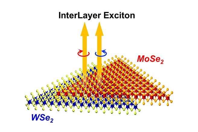
Scientists at the U.S. Naval Research Laboratory (NRL) have fabricated a bilayer structure comprised of two different monolayer materials, and observed a unique electronic state formed by the interaction between these two layers.
Transition metal dichalcogenides (TMDs), such as the inorganic compounds molybdenum diselenide (MoSe2) and tungsten diselenide (WSe2), are a class of layered 2-dimensional (2-D) materials akin to graphene. Novel heterostructures can be fabricated by stacking single monolayers of these materials and the properties can be tailored by the choice and sequence of these monolayers.
"Based on the experimental findings, we developed a new model of the interaction between these materials that has wide ranging implications for how they behave and how they can be used," said Dr. Aubrey Hanbicki, research physicists and lead author of the study. "We show how the interaction between the layers can alter their behavior to create a new composite system."
This new class of materials composed of atomically thin sheets has the potential to impact a wide range of technologies important to the Navy and the Department of Defense (DoD), states Dr. Berend T. Jonker, principal investigator of the effort. These range from chemical sensors to detect chemical warfare agents, explosives and toxic industrial chemicals, to novel optoelectronic devices for use in single-photon emitters, nano-lasers, photovoltaics, and photodetectors.
"In single layers, many TMDs are optically active semiconductors with some novel and exotic properties," Hanbicki explained. "When illuminated with light above a specific wavelength, dependent on the band gap of the material, electrons are excited from the valence band into the conduction band leaving a positively charged "hole" behind. The negatively charged electron and its hole are then attracted to each other and can form an electron-hole pair called an exciton. After a very brief time, they recombine and emit light at a wavelength characteristic of the material."
Typically, the lifetime of such excitons is very short. However, both the lifetime and emission wavelength can be tailored by judiciously selecting two dissimilar TMD monolayers to form a bilayer. With the right choice of materials, the electron and hole can reside in different layers. These spatially separated particles can form a so-called interlayer exciton (ILE), which takes a much longer time to recombine.
The interaction and subsequent recombination is highly dependent on the physical separation of the electron and hole, and considerable care must be taken to engineer the interface contact between the TMD layers.
The research at NRL used several advanced fabrication processes to stack and align single layer MoSe2flakes onto single layer WSe2. The MoSe2-WSe2 stack was further encapsulated by ultra-smooth hexagonal boron nitride (hBN) layers and then "cleaned" using a novel flattening technique recently developed by NRL scientists.
As a result, the ultraclean hBN/MoSe2-WSe2/hBN stack exhibits this unique interlayer exciton even at room temperature. At low temperatures, the ILE emission feature splits into two peaks providing the first clear resolution of this splitting, and enabling insight into the origin of the ILE itself. In particular, because the ILE peaks have nearly equal intensity, but opposite polarization, theoretical calculations can pinpoint the origin of the ILE.
"This work represents a significant advance in our general understanding of the interaction of TMDs in heterostructures and will inform the design and implementation of future TMD heterostructure devices," said Hanbicki.
These research results are reported in the journal ACS Nano
More information: Aubrey T. Hanbicki et al. Double Indirect Interlayer Exciton in a MoSe2/WSe2 van der Waals Heterostructure, ACS Nano (2018). DOI: 10.1021/acsnano.8b01369
Journal information: ACS Nano
Provided by Naval Research Laboratory


