On the cusp of valleytronics

Research into harnessing two-dimensional (2-D) materials for everyday devices has had some ups and downs. However, the emerging field of valleytronics is using energy troughs to offer renewed potential.
According to Johnson Goh, a senior scientist at A*STAR's Institute of Materials Research and Engineering, 2-D and other very thin materials could soon be using valleytronics to transmit information. Goh claims that a combination of increasingly affordable 2-D material production methods and the application of techniques such as valleytronics could quickly act together to shrink device sizes and power consumption needs.
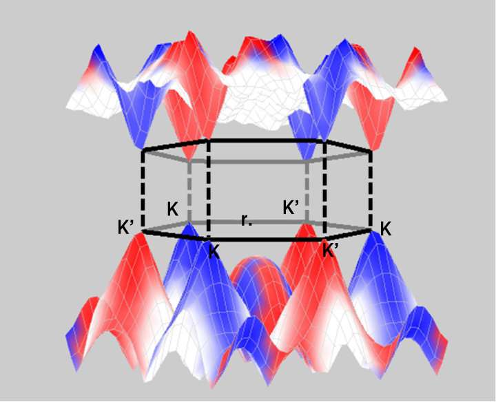
The basic idea is to pass information through 2-D and other very thin conducting materials using the energy 'valleys' (or energy extrema) in their conduction and valence bands (the energy bands around which electrons orbit an atom's nucleus). Information, says Goh, can be transmitted by controlling an electron's association with a valley—a manipulation that can be achieved using electric fields, magnetic fields and circularly polarised light.
For example, in molybdenum disulfide, which is a 2-D material, the presence of two inequivalent valleys means information can be stored in a binary manner based on which valley an electron is residing in: one valley could represent a zero, while the other could represent a one. This information can then be used for computation or memory.
Faster, better, stronger: 2-D semiconductors and valleytronics
Goh argues that a combination of valleytronics and 2-D or very thin materials will enable a whole host of functionalities in nanoelectronic and nanophotonic devices that can't be achieved with existing silicon-based semiconductor technology. For example, valleytronics would allow electron transport in 2-D materials to be manipulated at lower energies than conventional devices.
Information is transmitted in most of today's devices using a flow of charged electrons. In addition to often requiring more electrons to communicate, this method suffers from a 'crowding' of electrons and their jostling results in scattering and some loss of electron energy as heat. In valleytronics, on the other hand, scattering losses can be suppressed because electrons in energy valleys are somewhat protected from jostling.
Data can also be stored more robustly in valleytronics materials than in conventional data storage systems, Goh says. "The valley is a property of the whole material, and so the valley states are destroyed only if the material is significantly modified or ceases to exist," he explains. "So instead of encoding information onto electric charges that can be lost through scattering, encoding information onto valley states should be more enduring due to the unique coupling of electron spin to valley."
Currently, Goh and other researchers at IMRE are engineering a number of new and useful 2-D semiconductors for this technology by adjusting their composition to tune band gaps and thus control their conduction properties.
However, to create a binary information system using a 2-D material's valley states, it's also vital to differentiate which valley a charge is associated with using 'valley contrast'—which are opposite spins hosted by valleys with opposite indices. Transition-metal dichalcogenides, such as molybdenum disulfide, have proven useful to the team as these already have two distinct valleys with inherent contrast, eliminating the need to re-engineer these materials to have this property.

Goh and his team are also trying to add to the known list of materials with this key property. Over the past two years, in collaboration with the National University of Singapore, they have put together a suite of tools for sizing up 2-D materials for their valley contrast.
Large-area 2-D materials ready for the market
At the same time, Goh's colleagues are tackling one of the major obstacles to the commercialization of this technology. Finding reliable and scalable production methods for mass-scale electronics requires techniques that can form 2-D materials with uniform thickness and electrical properties over areas at least as large as a four-inch wafer: the standard substrate size used in the electronics industry.
To do this, Goh turned to IMRE colleague Dongzhi Chi, who is finding ways to manufacture large-area 2-D semiconductor materials using a method known as chemical vapor deposition. This technique forms materials by exposing a high-temperature substrate to gases carrying the desired atoms.
Chi and his team have already had some important success controlling the concentration spread of the chemical vapors of molybdenum disulfide during this process. By introducing a thin nickel oxide foam barrier trap to lower the chemical concentrations in the vapor, they have improved the uniformity and quality of the deposition material. "The advantage of this approach over others is ease," says Chi, "it uses chemical powders with low toxicity and minimal introduction of chemical species beyond the chemical elements in the deposited material itself, molybdenum and sulfur."
Proof of concept devices
Goh says his team is looking to demonstrate their first proof-of-concept devices by early 2019. He says these will include devices that use valleytronics to do simple things, such as switch a device on or off.
However, he adds that if valley electrons are put into superposition states they could produce a qubit—the fundamental unit for quantum computing. In fact, Goh sees the biggest future gains for valleytronics in its possible applications to "electronics such as low-power edge computing and eventually robust quantum computing."
Smaller devices mean smaller distances for information to travel and so valleytronics and quantum computing both offer advantages in data processing speeds. This has been noted by people trying to harness the spin of atoms for quantum computing. However, valleytronics may have an edge on spintronics as quantum spin is strongly linked to magnetic fields, which can introduce stability issues that aren't as problematic in valleytronics.
Because of this, Goh thinks making quantum computers that use valley states will be the key to opening up the whole 2-D material field for commercialization. "Quantum computing will help us showcase 2-D materials' advantages over classical electronics. If successful, companies could be more willing to invest in the infrastructure required to develop even better performing 2-D materials and turn them into truly disruptive technologies."
More information: Fabio Bussolotti et al. Roadmap on finding chiral valleys: screening 2D materials for valleytronics, Nano Futures (2018). DOI: 10.1088/2399-1984/aac9d7
Yee-Fun Lim et al. Modification of Vapor Phase Concentrations in MoS2 Growth Using a NiO Foam Barrier, ACS Nano (2018). DOI: 10.1021/acsnano.7b07682
Journal information: ACS Nano


