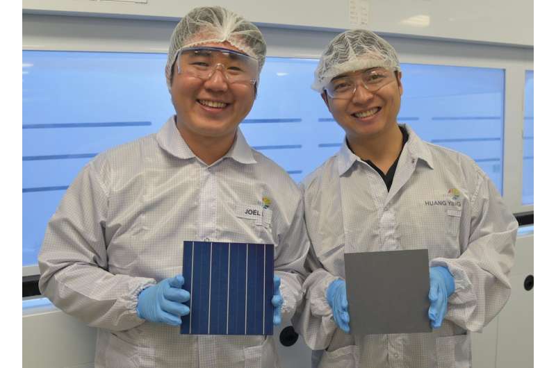
SERIS inventors holding textured DWS multicrystalline silicon solar cell and wafer. Credit: National University of Singapore
Scientists from the Solar Energy Research Institute of Singapore (SERIS) at the National University of Singapore (NUS) have developed a low-cost and effective technique to texture diamond-wire sawn (DWS) multicrystalline silicon (mc-Si) wafers. DWS wafers sliced using diamond-coated wires allow substantial cost savings compared to traditional slurry-cut wafers. Texturing is the process of roughening the silicon wafer surface so as to minimise front surface reflection and enhance light trapping, to boost the solar cell efficiency.
The solar industry has been in need of a cost-effective technique to texture these DWS mc-Si wafers. Current texturing technologies in the market are either too expensive or result in lower solar cell efficiencies.
To address this critical industrial problem, Dr. Joel Li's research group at SERIS has developed a wet-chemical technique to texture DWS mc-Si wafers effectively. The wet-chemical technique uses proprietary chemicals to etch the wafer surface such that nanoscale features with dimensions smaller than the incident light wavelength are formed. These nanoscale features greatly increase the chance of light having multiple bounces off the surface and being coupled into the wafer. The technique has the benefit of being low-cost, scalable and can be easily integrated into the processing tools of existing solar cell manufacturing plants. Dr. Li's research group has demonstrated the potential of this novel technology by processing mc-Si solar cells with efficiencies of 20%, which is about 0.5% (absolute) higher than those currently mass produced in the factories of tier-1 cell manufacturers.
"The two techniques that are commonly used to create a nanoscale texture on DWS mc-Si wafer surfaces are reactive ion etching (RIE) and metal-catalysed chemical etching (MCCE). The production costs of these two techniques are much higher than those of conventional acid-based texturing, and MCCE involves the use of metallic particles which runs the risk of introducing contaminants to production lines. Our technology is simpler, cheaper, metal-free and can achieve cell efficiencies of more than 20%. For these reasons, I strongly believe that our technology can become a mainstream texturing technology used by mc-Si solar cell manufacturers," said Dr. Huang Ying, the lead inventor of SERIS' DWS Wafer Texturing Technology.
This innovation marks a significant breakthrough, as it will allow the PV industry to improve module power while enjoying substantial cost savings through the use of cheaper DWS multicrystalline silicon wafers.
"We have addressed a long-standing challenge faced by the PV industry with our technology, and it has been proven to be an effective method for texturing DWS multicrystalline silicon wafers at low cost. The PV industry can leverage our technology to enable the switch from slurry-cut to cheaper DWS multicrystalline silicon wafers, which are 5-15% cheaper. For a gigawatt factory, this translates to cost savings in the order of US$10 million per year. In a cost-sensitive industry like PV, this level of cost savings is highly attractive," said Dr. Joel Li, Head of the Multicrystalline Silicon Wafer Solar Cell Group at SERIS.
"This low-cost texturing approach holds immense potential in facilitating substantial cost reduction for the PV industry, and it has already been recognised by several tier-1 manufacturers. SERIS plans to license the technology to interested manufacturers and work closely with them to implement and scale up the texturing process on their production lines. As the PV industry experiences a major shift from slurry-cut to DWS mc-Si wafers this year, we believe that this novel technology developed by SERIS will become a mainstream texturing technology for DWS mc-Si wafers," said SERIS CEO Prof Armin Aberle.
Provided by National University of Singapore


