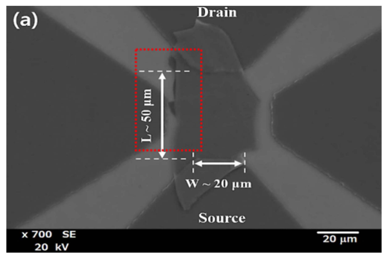
Scanning electron microscopy image of the near-infrared photodetector based on few-layered MoSe2. Credit: University of Electro Communications
Optical sensors operating in the near infrared (NIR) are important for applications in imaging, photodetectors, and biological sensors. Notably, recent reports on the synthesis of high quality, large areas of graphene has motivated researchers to search for other 2-D materials with properties suitable for NIR devices.
Now, Abdelkader Abderrahmane and colleagues at the University of Electro-Communications, Tokyo in collaboration with researchers at Chosun University, Korea, describe the optoelectronics characteristics of molybdenum selenide (MoSe2) phototransistors for applications to photodetectors. The application of gate voltages to the devices yielded a maximum photoresponsivity 238 A/W, an external quantum efficiency (EQE) of 37,745% under 785 nm light. The researchers state: "our device is one of the best high-performance nanoscale near-infrared photodetectors based on multilayered two-dimensional materials."
The devices were fabricated using few layered MoSe2 with a thickness of ~44 nm that was exfoliated from natural MoSe2 onto thermally oxidized silicon substrates with metallic strips acting as back gates. The transistor channel width and length were 50 and 20 μm, and the charge mobility was be 5.1 cm2 /V/s.
Electrical measurements indicated that the devices operated in the so-called accumulation mode and with a pinch off voltage of - 40V.
The combination of the 1.1 eV bandgap of MoSe2 and its high optical absorption compared to MoS2 is expected to offer wide ranging applications in optoelectronics.
More information: Pil Ju Ko et al. High-performance near-infrared photodetector based on nano-layered MoSe2, Semiconductor Science and Technology (2017). DOI: 10.1088/1361-6641/aa6819
Journal information: Semiconductor Science and Technology
Provided by University of Electro Communications


