December 20, 2016 report
Synthesis of pseudo-1D semiconductor provides insight into anisotropic 2D materials

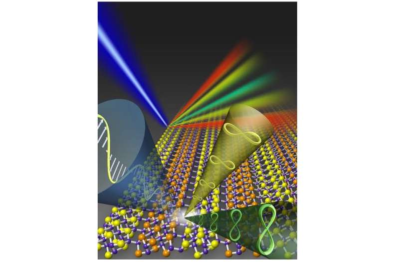
(Phys.org)—For the first time, researchers have synthesized semiconducting gallium telluride (GaTe) in the monoclinic phase as a pseudo-one-dimensional (pseudo-1D) material. This new class of materials is characterized by quasi-1D chains of atoms running in a particular direction along a 2D surface.
The researchers, led by Sefaattin Tongay, Assistant Professor of Materials Science and Engineering at Arizona State University, have published a paper on the first synthesis of the pseudo-1D GaTe material in a recent issue of Advanced Materials.
"This is the first demonstration of the synthesis of anisotropic GaTe nanomaterials," Tongay told Phys.org. "In addition to these novel synthesis efforts, we have also provided the first atomic insight into how atoms in two dimensions arrange themselves into pseudo-1D chains within the plane, and investigated their anisotropic optical properties."
So far, research in this area has remained limited, with only a few studies having investigated GaTe by isolating 2D monolayers from bulk crystals. The current work offers novel routes to large-scale synthesis and hints at exciting new phenomena.
Synthesizing GaTe in the pseudo-1D form has been challenging because of the material's large crystalline anisotropy. Here, the researchers used a physical vapor transport technique in which high temperatures and low pressures in a tube furnace transform the semiconductor powder into its pseudo-1D form.
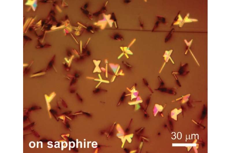
One particularly interesting property arising from the unique crystal structure of the new form of GaTe is that the atomic chains divide each individual GaTe flake into a bowtie shape consisting of four separate domains with different crystal orientations.
In each of these different domains, the material has a different chain orientation, resulting in different anisotropic behavior. For instance, experiments revealed that the maximum light emission intensity differs depending on the domain, offering a path toward developing photonics applications.
The researchers demonstrated the scalable growth of pseudo-1D GaTe on three different industrially compatible substrates, and found that the morphology of the GaTe nanostructures strongly depends on the substrate.

For instance, they found that GaTe chains grow much more randomly on sapphire than on silicon and gallium arsenide, with the result that GaTe atoms lying on the sapphire surface can move around much more freely.
The GaTe nanostructures on sapphire also have certain defects that cause a highly efficient, narrow optical emission peak below the band edge emission, which is unlike the broad defect emissions normally found in semiconductors.
The result that the pseudo-1D GaTe is the only known form of GaTe to emit bright luminescence below the optical bandgap may offer a starting point for defect engineering for optoelectronics applications.
"I think the greatest significance lies in the discovery of the multi-color emission, especially the sharp sub-band emission that does not look like a defect emission at all," said coauthor Hui Cai, a PhD student at Arizona State University. "These emissions may originate from intermediate bands, which has been given much attention in ZnTeO and CuGaS2 but never in GaTe. This may be the first experimental fingerprint that intermediate bands also exist in GaTe with certain kinds of defects."
The researchers expect that, given its unique optical properties, pseudo-1D GaTe may have a variety of future applications.
"Due to the existence of optically active states below the gap, the synthesized GaTe can be a potential candidate for intermediate band solar cells," Cai said. "It can capture photons in the near-infrared range, the energy of which is lower than its bandgap. Beside this, it absorbs light polarized along its chain direction and is transparent to light polarized perpendicular to that direction. Thus it has potential applications in linear polarizers and polarized photodetectors."
The new material also has potential applications for the polarized light industry.
"These materials offer unique properties that bridge many kinds of one-dimensional materials, like carbon nanotubes, nanowires, etc., and conventional 2D materials such as graphene, MoS2, and GaSe," Tongay said. "Because of their large crystalline anisotropy and anisotropic physical properties, they can potentially offer polarization-sensitive optical properties, dichroism, highly conductive electronic carriers, and high thermal conduction along their anisotropy direction. We anticipate that polarization-sensitive photonic applications, single photon emitters, and high-electron mobility transistors are likely to emerge from these materials."
More information: Hui Cai et al. "Synthesis of Highly Anisotropic Semiconducting GaTe Nanomaterials and Emerging Properties Enabled by Epitaxy." Advanced Materials. DOI: 10.1002/adma.201605551
Journal information: Advanced Materials
© 2016 Phys.org


