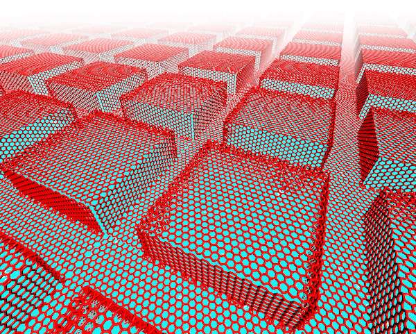
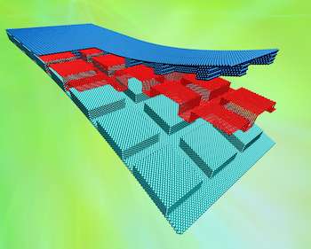
Rice University researchers used computer models to determine the best way to disperse heat produced by microelectronic devices using gallium nitride semiconductors and diamond. A patterned surface and a layer of atom-thick graphene helped transport phonons from the semiconductor to the heat sink. Credit: Lei Tao
Bumpy surfaces with graphene between would help dissipate heat in next-generation microelectronic devices, according to Rice University scientists.
Their theoretical studies show that enhancing the interface between gallium nitride semiconductors and diamond heat sinks would allow phonons – quasiparticles of sound that also carry heat – to disperse more efficiently. Heat sinks are used to carry heat away from electronic devices.
Rice computer models replaced the flat interface between the materials with a nanostructured pattern and added a layer of graphene, the atom-thick form of carbon, as a way to dramatically improve heat transfer, said Rice materials scientist Rouzbeh Shahsavari.
The new work by Shahsavari, Rice graduate student and lead author Lei Tao and postdoctoral researcher Sreeprasad Sreenivasan appeared this month in the American Chemical Society journal ACS Applied Materials and Interfaces.
No matter the size, electronic devices need to disperse the heat they produce, Shahsavari said. "With the current trend of constant increases in power and device miniaturization, efficient heat management has become a serious issue for reliability and performance," he said. "Oftentimes, the individual materials in hybrid nano- and microelectronic devices function well but the interface of different materials is the bottleneck for heat diffusion."
Gallium nitride has become a strong candidate for use in high-power, high-temperature applications like uninterruptible power supplies, motors, solar converters and hybrid vehicles, he said. Diamond is an excellent heat sink, but its atomic interface with gallium nitride is hard for phonons to traverse.
Rice simulations show that graphene between patterned gallium nitride and diamond would offer excellent heat transfer in next-generation hybrids of nano- and microelectronics. Credit: Lei Tao
The researchers simulated 48 distinct grid patterns with square or round graphene pillars and tuned them to match phonon vibration frequencies between the materials. Sinking a dense pattern of small squares into the diamond showed a dramatic decrease in thermal boundary resistance of up to 80 percent. A layer of graphene between the materials further reduced resistance by 33 percent.
Fine-tuning the pillar length, size, shape, hierarchy, density and order will be important, Lei said.
"With current and emerging advancements in nanofabrication like nanolithography, it is now possible to go beyond the conventional planer interfaces and create strategically patterned interfaces coated with nanomaterials to significantly boost heat transport," Shahsavari said. "Our strategy is amenable to several other hybrid materials and provides novel insights to overcome the thermal boundary resistance bottleneck."
Shahsavari is an assistant professor of civil and environmental engineering and of materials science and nanoengineering.
The researchers used the Blue Gene supercomputer and the National Science Foundation-supported DAVinCI supercomputer, which are both administered by Rice's Center for Research Computing and were procured in partnership with Rice's Ken Kennedy Institute for Information Technology.
More information: Lei Tao et al. Interlaced, Nanostructured Interface with Graphene Buffer Layer Reduces Thermal Boundary Resistance in Nano/microelectronic Systems, ACS Applied Materials & Interfaces (2016). DOI: 10.1021/acsami.6b09482
Journal information: ACS Applied Materials and Interfaces
Provided by Rice University


